- 您現(xiàn)在的位置:買賣IC網(wǎng) > PDF目錄30981 > MQSMBG5931AE3 (MICROSEMI CORP-SCOTTSDALE) 18 V, 1.25 W, SILICON, UNIDIRECTIONAL VOLTAGE REGULATOR DIODE, DO-215AA PDF資料下載
參數(shù)資料
| 型號: | MQSMBG5931AE3 |
| 廠商: | MICROSEMI CORP-SCOTTSDALE |
| 元件分類: | 齊納二極管 |
| 英文描述: | 18 V, 1.25 W, SILICON, UNIDIRECTIONAL VOLTAGE REGULATOR DIODE, DO-215AA |
| 封裝: | ROHS COMPLIANT, PLASTIC, SMBG, 2 PIN |
| 文件頁數(shù): | 1/3頁 |
| 文件大?。?/td> | 122K |
| 代理商: | MQSMBG5931AE3 |

SILICON 2.0 Watt ZENER DIODES
WWW
.Microse
m
i
.CO
M
S C O T TS DALE DIVISION
SMBG5913 thru SMBG5956B, e3
SMBJ5913 thru SMBJ5956B, e3
SMBG
(J)591
3–59
56
B,
e3
DESCRIPTION
APPEARANCE
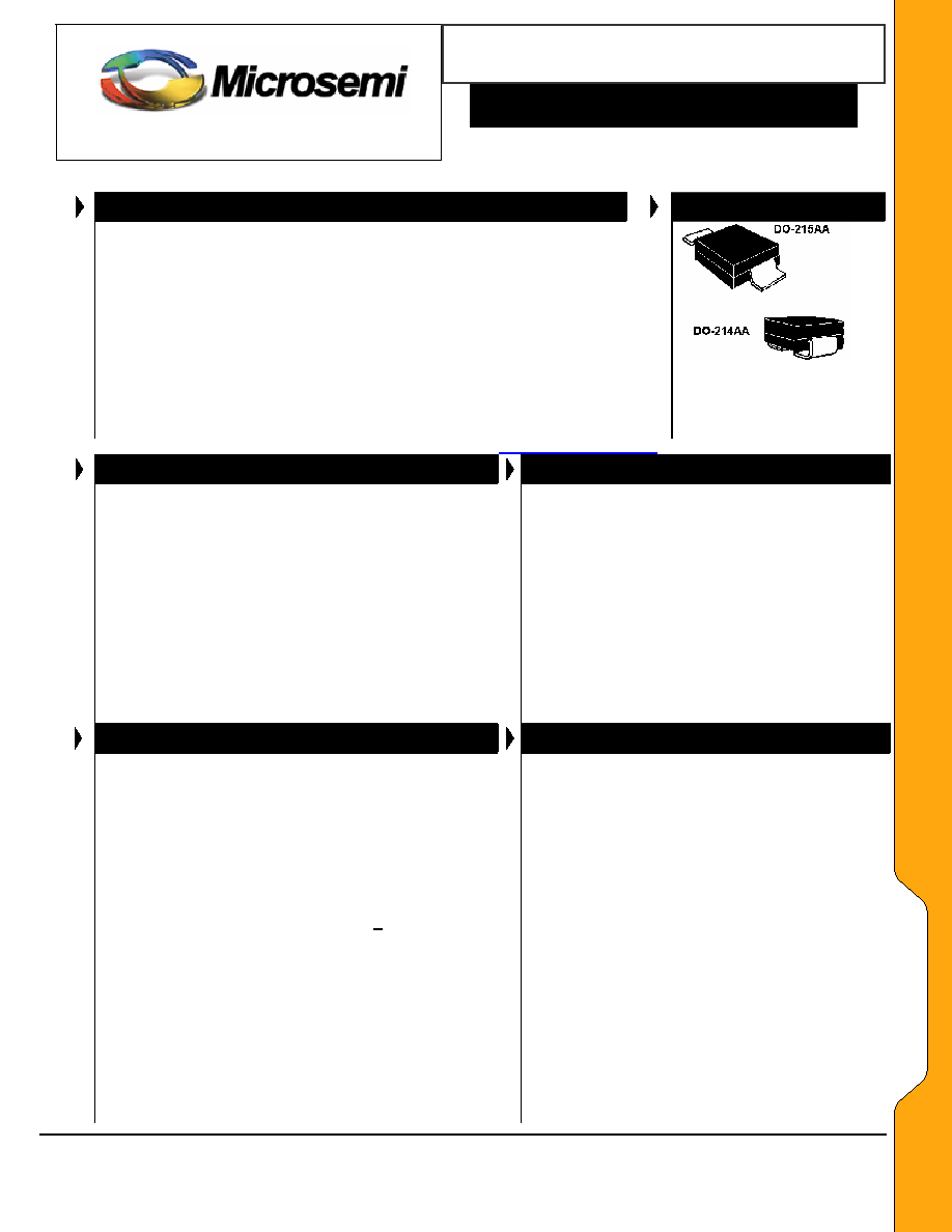
The SMBJ5913-5956B or SMBG5913-5956B series of surface mount 2.0
watt Zeners provides voltage regulation in a selection from 3.3 to 200
volts with different tolerances as identified by suffix letter on the part
number. This series is equivalent to the JEDEC registered 1N5913 thru
1N5956B with identical electrical characteristics except it is rated at 2.0 W
instead of 1.5 W with the lower thermal resistance features of the surface
mount packaging. It is available in J-bend design (SMBJ) with the DO-
214AA package for greater PC board mounting density or in Gull-wing
design (SMBG) in the DO-215AA for visible solder connections. It is also
available as RoHS Compliant with an e3 suffix. Microsemi also offers
numerous other Zener products to meet higher and lower power
applications.
NOTE: All SMB series are
equivalent to prior SMS package
identifications.
IMPORTANT: For the most current data, consult MICROSEMI’s website: http://www.microsemi.com
FEATURES
APPLICATIONS / BENEFITS
Surface mount equivalent to 1N5913 to 1N5956B
Ideal for high-density and low-profile mounting
Zener voltage available 3.3V to 200V
Standard voltage tolerances are plus/minus 5% with
B suffix and 10 % with A suffix identification
Tight tolerances available in plus or minus 2% or 1%
with C or D suffix respectively
Options for screening in accordance with MIL-PRF-19500
for JAN, JANTX, and JANTXV are available by adding MQ,
MX, or MV prefixes respectively to part numbers.
RoHS Compliant devices available by adding an “e3” suffix
Regulates voltage over a broad operating
current and temperature range
Wide selection from 3.3 to 200 V
Popular DO-214AA or DO-215AA packages
and footprints for either high density J-bend or
Gull-wing designs for visible solder joints
Nonsensitive to ESD per MIL-STD-750 Method
1020
Withstands high surge stresses (see Figure 2)
Moisture classification: Level 1 per IPC/JEDEC
J-STD-020B with no dry pack required
MAXIMUM RATINGS
MECHANICAL AND PACKAGING
Power dissipation at 25C: 2.0 watts (also see
derating in Figure 1).
Operating and Storage temperature: -65C to
+150
C
Thermal Resistance: 35 C/W junction to lead, or
100
C/W junction to ambient when mounted on FR4
PC board (1oz Cu) with recommended footprint (see
last page)
Steady-State Power: 2 watts at T
L < 80
oC, or 1.25
watts at TA = 25
C when mounted on FR4 PC board
with recommended footprint (also see Figure 1)
Forward voltage @200 mA: 1.2 volts (maximum)
Solder Temperatures: 260 C for 10 s (maximum)
CASE: Void-free transfer molded
thermosetting epoxy body meeting UL94V-0
TERMINALS: Gull-wing or C-bend (modified
J-bend) tin-lead or RoHS compliant annealed
matte-Tin plating solderable per MIL-STD-750,
method 2026
POLARITY: Cathode indicated by band.
Diode to be operated with banded end positive
with respect to opposite end for Zener
regulation
MARKING: Includes part number without
prefix (e.g. 5913B, 5913Be3, 5948C, 5956D,
etc.)
TAPE & REEL option: Standard per EIA-481-1-
A
with 12 mm tape, 750 per 7 inch reel or 2500
per 13 inch reel (add “TR” suffix to part number)
WEIGHT: 0.1 grams
See package dimensions on last page
Microsemi
Scottsdale Division
Page 1
Copyright
2007
6-21--2007 REV H
8700 E. Thomas Rd. PO Box 1390, Scottsdale, AZ 85252 USA, (480) 941-6300, Fax: (480) 947-1503
相關(guān)PDF資料 |
PDF描述 |
|---|---|
| MQSMBG5931BE3 | 18 V, 1.25 W, SILICON, UNIDIRECTIONAL VOLTAGE REGULATOR DIODE, DO-215AA |
| MQSMBG5931DE3 | 18 V, 1.25 W, SILICON, UNIDIRECTIONAL VOLTAGE REGULATOR DIODE, DO-215AA |
| MQSMBG5931E3 | 18 V, 1.25 W, SILICON, UNIDIRECTIONAL VOLTAGE REGULATOR DIODE, DO-215AA |
| MQSMBG5932AE3 | 20 V, 1.25 W, SILICON, UNIDIRECTIONAL VOLTAGE REGULATOR DIODE, DO-215AA |
| MQSMBG5932DE3 | 20 V, 1.25 W, SILICON, UNIDIRECTIONAL VOLTAGE REGULATOR DIODE, DO-215AA |
相關(guān)代理商/技術(shù)參數(shù) |
參數(shù)描述 |
|---|---|
| MQSMCGLCE10 | 制造商:MICROSEMI 制造商全稱:Microsemi Corporation 功能描述:1500 WATT LOW CAPACITANCE SURFACE MOUNT TRANSIENT VOLTAGE SUPPRESSOR |
| MQSMCGLCE100 | 制造商:MICROSEMI 制造商全稱:Microsemi Corporation 功能描述:1500 WATT LOW CAPACITANCE SURFACE MOUNT TRANSIENT VOLTAGE SUPPRESSOR |
| MQSMCGLCE100A | 制造商:MICROSEMI 制造商全稱:Microsemi Corporation 功能描述:1500 WATT LOW CAPACITANCE SURFACE MOUNT TRANSIENT VOLTAGE SUPPRESSOR |
| MQSMCGLCE100ATR | 制造商:MICROSEMI 制造商全稱:Microsemi Corporation 功能描述:1500 WATT LOW CAPACITANCE SURFACE MOUNT TRANSIENT VOLTAGE SUPPRESSOR |
| MQSMCGLCE100TR | 制造商:MICROSEMI 制造商全稱:Microsemi Corporation 功能描述:1500 WATT LOW CAPACITANCE SURFACE MOUNT TRANSIENT VOLTAGE SUPPRESSOR |
發(fā)布緊急采購,3分鐘左右您將得到回復(fù)。