- 您現(xiàn)在的位置:買賣IC網(wǎng) > PDF目錄25636 > MQ80C52TXXX-16:D (ATMEL CORP) 8-BIT, MROM, 16 MHz, MICROCONTROLLER, CQFP44 PDF資料下載
參數(shù)資料
| 型號: | MQ80C52TXXX-16:D |
| 廠商: | ATMEL CORP |
| 元件分類: | 微控制器/微處理器 |
| 英文描述: | 8-BIT, MROM, 16 MHz, MICROCONTROLLER, CQFP44 |
| 封裝: | CERAMIC, QFP-44 |
| 文件頁數(shù): | 41/134頁 |
| 文件大?。?/td> | 3805K |
第1頁第2頁第3頁第4頁第5頁第6頁第7頁第8頁第9頁第10頁第11頁第12頁第13頁第14頁第15頁第16頁第17頁第18頁第19頁第20頁第21頁第22頁第23頁第24頁第25頁第26頁第27頁第28頁第29頁第30頁第31頁第32頁第33頁第34頁第35頁第36頁第37頁第38頁第39頁第40頁當(dāng)前第41頁第42頁第43頁第44頁第45頁第46頁第47頁第48頁第49頁第50頁第51頁第52頁第53頁第54頁第55頁第56頁第57頁第58頁第59頁第60頁第61頁第62頁第63頁第64頁第65頁第66頁第67頁第68頁第69頁第70頁第71頁第72頁第73頁第74頁第75頁第76頁第77頁第78頁第79頁第80頁第81頁第82頁第83頁第84頁第85頁第86頁第87頁第88頁第89頁第90頁第91頁第92頁第93頁第94頁第95頁第96頁第97頁第98頁第99頁第100頁第101頁第102頁第103頁第104頁第105頁第106頁第107頁第108頁第109頁第110頁第111頁第112頁第113頁第114頁第115頁第116頁第117頁第118頁第119頁第120頁第121頁第122頁第123頁第124頁第125頁第126頁第127頁第128頁第129頁第130頁第131頁第132頁第133頁第134頁
14
8068U–AVR–06/2013
XMEGA A3
Not recommended for new designs -
Use XMEGA A3U series
7.7
Flash and EEPROM Page Size
The Flash Program Memory and EEPROM data memory are organized in pages. The pages are
word accessible for the Flash and byte accessible for the EEPROM.
Table 7-2 on page 14 shows the Flash Program Memory organization. Flash write and erase
operations are performed on one page at a time, while reading the Flash is done one byte at a
time. For Flash access the Z-pointer (Z[m:n]) is used for addressing. The most significant bits in
the address (FPAGE) gives the page number and the least significant address bits (FWORD)
gives the word in the page.
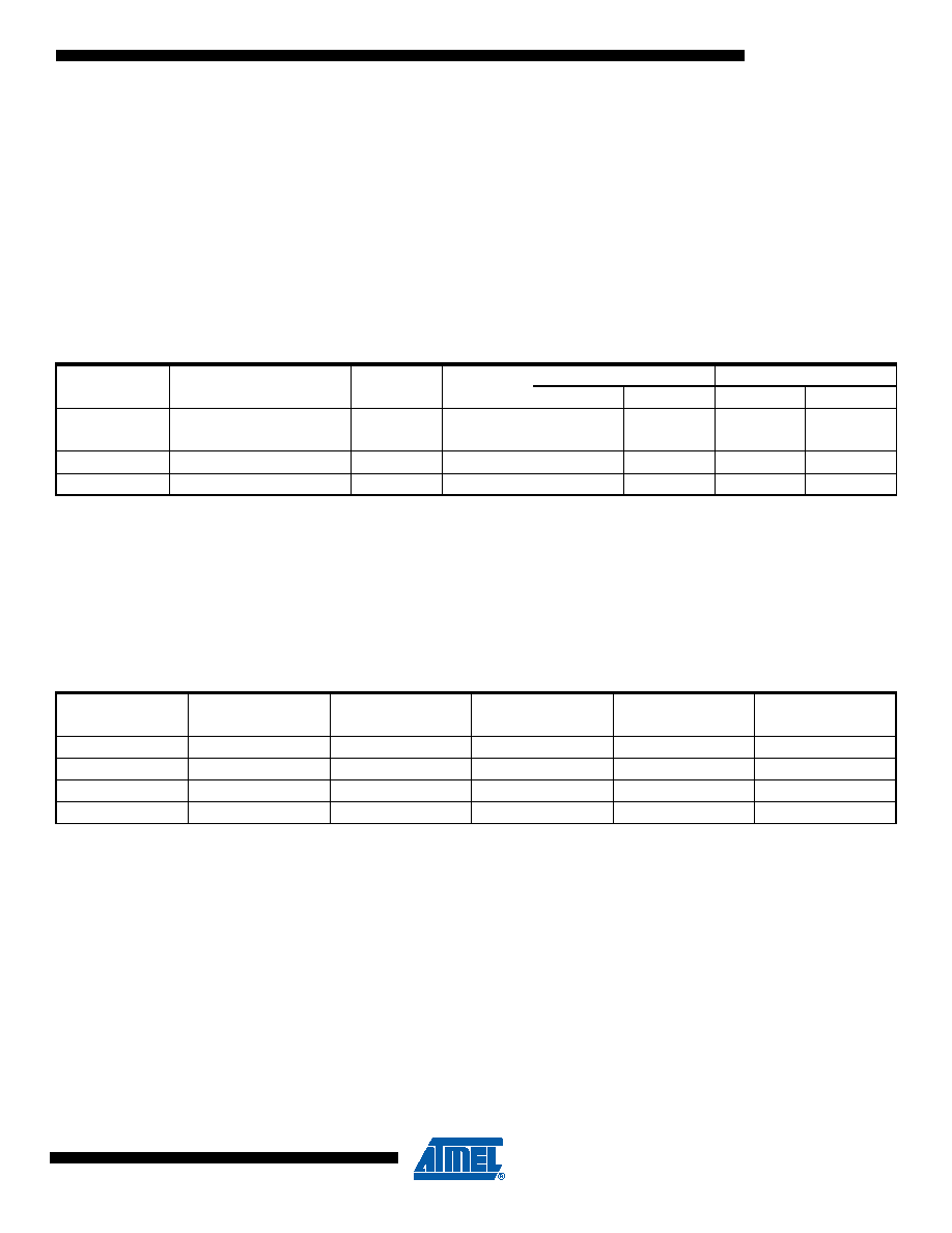
Table 7-2.
Number of words and Pages in the Flash.
Table 7-3 on page 14 shows EEPROM memory organization for the XMEGA A3 devices. EEE-
PROM write and erase operations can be performed one page or one byte at a time, while
reading the EEPROM is done one byte at a time. For EEPROM access the NVM Address Regis-
ter (ADDR[m:n]) is used for addressing. The most significant bits in the address (E2PAGE) gives
Table 7-3.
Number of bytes and Pages in the EEPROM.
Devices
Flash
Page Size
FWORD
FPAGE
Application
Boot
Size
(words)
Size
No of Pages
Size
No of Pages
ATxmega64A3
64 KB + 4 KB
128
Z[7:1]
Z[16:8]
64K
256
4 KB
16
ATxmega128A3
128 KB + 8 KB
256
Z[8:1]
Z[17:9]
128K
256
8 KB
16
ATxmega192A3
192 KB + 8 KB
256
Z[8:1]
Z[18:9]
192K
384
8 KB
16
ATxmega256A3
256 KB + 8 KB
256
Z[8:1]
Z[18:9]
256K
512
8 KB
16
Devices
EEPROM
Page Size
E2BYTE
E2PAGE
No of Pages
Size
(Bytes)
ATxmega64A3
2 KB
32
ADDR[4:0]
ADDR[10:5]
64
ATxmega128A3
2 KB
32
ADDR[4:0]
ADDR[10:5]
64
ATxmega192A3
2 KB
32
ADDR[4:0]
ADDR[10:5]
64
ATxmega256A3
4 KB
32
ADDR[4:0]
ADDR[11:5]
128
相關(guān)PDF資料 |
PDF描述 |
|---|---|
| S83C154CXXX-36 | 8-BIT, MROM, 36 MHz, MICROCONTROLLER, PQCC44 |
| S80C52EXXX-16R | 8-BIT, MROM, 16 MHz, MICROCONTROLLER, PQCC44 |
| MR80C52TXXX-16P883D | 8-BIT, MROM, 16 MHz, MICROCONTROLLER, CQCC44 |
| MC80C32-25SCD | 8-BIT, 25 MHz, MICROCONTROLLER, CDIP40 |
| MQ80C32E-25SHXXX:R | 8-BIT, 25 MHz, MICROCONTROLLER, CQFP44 |
相關(guān)代理商/技術(shù)參數(shù) |
參數(shù)描述 |
|---|---|
| MQ82370-20 | 制造商:Rochester Electronics LLC 功能描述:- Bulk |
| MQ8238020 | 制造商:Intel 功能描述:CONTROLLER: OTHER |
| MQ82380-20 | 制造商:Rochester Electronics LLC 功能描述:- Bulk |
| MQ82380-20/R | 制造商:Rochester Electronics LLC 功能描述: |
| MQ82592 | 制造商:Rochester Electronics LLC 功能描述:- Bulk |
發(fā)布緊急采購,3分鐘左右您將得到回復(fù)。