- 您現(xiàn)在的位置:買賣IC網(wǎng) > PDF目錄25636 > MQ80C32E-30/883:RD (TEMIC SEMICONDUCTORS) 8-BIT, 30 MHz, MICROCONTROLLER, CQFP44 PDF資料下載
參數(shù)資料
| 型號: | MQ80C32E-30/883:RD |
| 廠商: | TEMIC SEMICONDUCTORS |
| 元件分類: | 微控制器/微處理器 |
| 英文描述: | 8-BIT, 30 MHz, MICROCONTROLLER, CQFP44 |
| 文件頁數(shù): | 161/392頁 |
| 文件大?。?/td> | 6486K |
第1頁第2頁第3頁第4頁第5頁第6頁第7頁第8頁第9頁第10頁第11頁第12頁第13頁第14頁第15頁第16頁第17頁第18頁第19頁第20頁第21頁第22頁第23頁第24頁第25頁第26頁第27頁第28頁第29頁第30頁第31頁第32頁第33頁第34頁第35頁第36頁第37頁第38頁第39頁第40頁第41頁第42頁第43頁第44頁第45頁第46頁第47頁第48頁第49頁第50頁第51頁第52頁第53頁第54頁第55頁第56頁第57頁第58頁第59頁第60頁第61頁第62頁第63頁第64頁第65頁第66頁第67頁第68頁第69頁第70頁第71頁第72頁第73頁第74頁第75頁第76頁第77頁第78頁第79頁第80頁第81頁第82頁第83頁第84頁第85頁第86頁第87頁第88頁第89頁第90頁第91頁第92頁第93頁第94頁第95頁第96頁第97頁第98頁第99頁第100頁第101頁第102頁第103頁第104頁第105頁第106頁第107頁第108頁第109頁第110頁第111頁第112頁第113頁第114頁第115頁第116頁第117頁第118頁第119頁第120頁第121頁第122頁第123頁第124頁第125頁第126頁第127頁第128頁第129頁第130頁第131頁第132頁第133頁第134頁第135頁第136頁第137頁第138頁第139頁第140頁第141頁第142頁第143頁第144頁第145頁第146頁第147頁第148頁第149頁第150頁第151頁第152頁第153頁第154頁第155頁第156頁第157頁第158頁第159頁第160頁當前第161頁第162頁第163頁第164頁第165頁第166頁第167頁第168頁第169頁第170頁第171頁第172頁第173頁第174頁第175頁第176頁第177頁第178頁第179頁第180頁第181頁第182頁第183頁第184頁第185頁第186頁第187頁第188頁第189頁第190頁第191頁第192頁第193頁第194頁第195頁第196頁第197頁第198頁第199頁第200頁第201頁第202頁第203頁第204頁第205頁第206頁第207頁第208頁第209頁第210頁第211頁第212頁第213頁第214頁第215頁第216頁第217頁第218頁第219頁第220頁第221頁第222頁第223頁第224頁第225頁第226頁第227頁第228頁第229頁第230頁第231頁第232頁第233頁第234頁第235頁第236頁第237頁第238頁第239頁第240頁第241頁第242頁第243頁第244頁第245頁第246頁第247頁第248頁第249頁第250頁第251頁第252頁第253頁第254頁第255頁第256頁第257頁第258頁第259頁第260頁第261頁第262頁第263頁第264頁第265頁第266頁第267頁第268頁第269頁第270頁第271頁第272頁第273頁第274頁第275頁第276頁第277頁第278頁第279頁第280頁第281頁第282頁第283頁第284頁第285頁第286頁第287頁第288頁第289頁第290頁第291頁第292頁第293頁第294頁第295頁第296頁第297頁第298頁第299頁第300頁第301頁第302頁第303頁第304頁第305頁第306頁第307頁第308頁第309頁第310頁第311頁第312頁第313頁第314頁第315頁第316頁第317頁第318頁第319頁第320頁第321頁第322頁第323頁第324頁第325頁第326頁第327頁第328頁第329頁第330頁第331頁第332頁第333頁第334頁第335頁第336頁第337頁第338頁第339頁第340頁第341頁第342頁第343頁第344頁第345頁第346頁第347頁第348頁第349頁第350頁第351頁第352頁第353頁第354頁第355頁第356頁第357頁第358頁第359頁第360頁第361頁第362頁第363頁第364頁第365頁第366頁第367頁第368頁第369頁第370頁第371頁第372頁第373頁第374頁第375頁第376頁第377頁第378頁第379頁第380頁第381頁第382頁第383頁第384頁第385頁第386頁第387頁第388頁第389頁第390頁第391頁第392頁
243
2552K–AVR–04/11
ATmega329/3290/649/6490
23.4.4
LCDCCR – LCD Contrast Control Register
Bits 7:5 – LCDDC2:0: LDC Display Configuration
The LCDDC2:0 bits determine the amount of time the LCD drivers are turned on for each volt-
age transition on segment and common pins. A short drive time will lead to lower power
consumption, but displays with high internal resistance may need longer drive time to achieve
satisfactory contrast. Note that the drive time will never be longer than one half prescaled LCD
clock period, even if the selected drive time is longer. When using static duty or blanking, drive
time will always be one half prescaled LCD clock period.
New values take effect immediately, and can cause small glitches in the display output. This can
be avoided by setting the LCDBL in LCDCRA, and wait to the next start of frame before chang-
ing LCDDC2:0.
Note:
The drive time will be longer dependent on oscillator startup time.
Bit 4 – Reserved Bit
This bit is reserved in the ATmega329/3290/649/6490 and will always read as zero.
Bits 3:0 – LCDCC3:0: LCD Contrast Control
The LCDCC3:0 bits determine the maximum voltage V
LCD on segment and common pins. The
different selections are shown in Table 23-8. New values take effect every beginning of a new
frame.
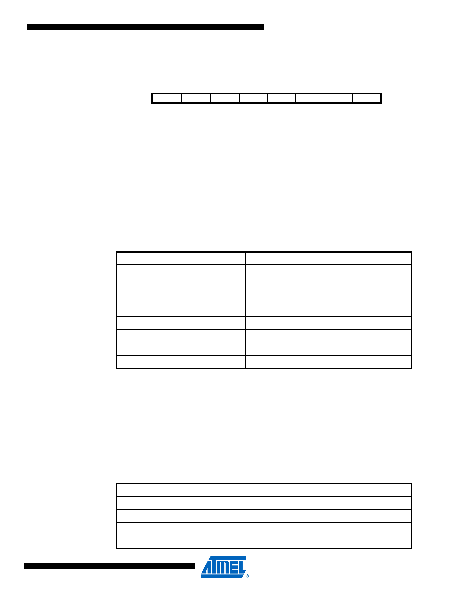
Bit
765
4
3
2
1
0
LCDDC2
LCDDC1
LCDDC0
–
LCDCC3
LCDCC2
LCDCC1
LCDCC0
LCDCCR
Read/Write
R/W
R
R/W
Initial Value
0
Table 23-7.
LCD Display Configuration
LCDDC2
LCDDC1
LCDDC0
Nominal drive time
0
300s
0
1
70s
0
1
0
150s
0
1
450s
1
0
575s
101
850s
1
0
1150s
111
50% of clk
LCD_PS
Table 23-8.
LCD Contrast Control
LCDCC3
LCDCC2
LCDCC1
LCDCC0
Maximum Voltage V
LCD
0
2.60
0
1
2.65
0
1
0
2.70
0
1
2.75
相關PDF資料 |
PDF描述 |
|---|---|
| MD80C32E-12SBD | 8-BIT, 12 MHz, MICROCONTROLLER, CDIP40 |
| MC80C32E-20P883D | 8-BIT, 20 MHz, MICROCONTROLLER, CDIP40 |
| MR83C154CXXX-20P883D | 8-BIT, MROM, 20 MHz, MICROCONTROLLER, CQCC44 |
| MQ83C154TXXX-30/883R | 8-BIT, MROM, 30 MHz, MICROCONTROLLER, CQFP44 |
| MR83C154TXXX-36P883 | 8-BIT, MROM, 36 MHz, MICROCONTROLLER, CQCC44 |
相關代理商/技術參數(shù) |
參數(shù)描述 |
|---|---|
| MQ82370-20 | 制造商:Rochester Electronics LLC 功能描述:- Bulk |
| MQ8238020 | 制造商:Intel 功能描述:CONTROLLER: OTHER |
| MQ82380-20 | 制造商:Rochester Electronics LLC 功能描述:- Bulk |
| MQ82380-20/R | 制造商:Rochester Electronics LLC 功能描述: |
| MQ82592 | 制造商:Rochester Electronics LLC 功能描述:- Bulk |
發(fā)布緊急采購,3分鐘左右您將得到回復。