- 您現(xiàn)在的位置:買賣IC網(wǎng) > PDF目錄25632 > MQ80C32-20P883 (TEMIC SEMICONDUCTORS) 8-BIT, 20 MHz, MICROCONTROLLER, CQFP44 PDF資料下載
參數(shù)資料
| 型號(hào): | MQ80C32-20P883 |
| 廠商: | TEMIC SEMICONDUCTORS |
| 元件分類: | 微控制器/微處理器 |
| 英文描述: | 8-BIT, 20 MHz, MICROCONTROLLER, CQFP44 |
| 文件頁(yè)數(shù): | 166/310頁(yè) |
| 文件大小: | 4427K |
| 代理商: | MQ80C32-20P883 |
第1頁(yè)第2頁(yè)第3頁(yè)第4頁(yè)第5頁(yè)第6頁(yè)第7頁(yè)第8頁(yè)第9頁(yè)第10頁(yè)第11頁(yè)第12頁(yè)第13頁(yè)第14頁(yè)第15頁(yè)第16頁(yè)第17頁(yè)第18頁(yè)第19頁(yè)第20頁(yè)第21頁(yè)第22頁(yè)第23頁(yè)第24頁(yè)第25頁(yè)第26頁(yè)第27頁(yè)第28頁(yè)第29頁(yè)第30頁(yè)第31頁(yè)第32頁(yè)第33頁(yè)第34頁(yè)第35頁(yè)第36頁(yè)第37頁(yè)第38頁(yè)第39頁(yè)第40頁(yè)第41頁(yè)第42頁(yè)第43頁(yè)第44頁(yè)第45頁(yè)第46頁(yè)第47頁(yè)第48頁(yè)第49頁(yè)第50頁(yè)第51頁(yè)第52頁(yè)第53頁(yè)第54頁(yè)第55頁(yè)第56頁(yè)第57頁(yè)第58頁(yè)第59頁(yè)第60頁(yè)第61頁(yè)第62頁(yè)第63頁(yè)第64頁(yè)第65頁(yè)第66頁(yè)第67頁(yè)第68頁(yè)第69頁(yè)第70頁(yè)第71頁(yè)第72頁(yè)第73頁(yè)第74頁(yè)第75頁(yè)第76頁(yè)第77頁(yè)第78頁(yè)第79頁(yè)第80頁(yè)第81頁(yè)第82頁(yè)第83頁(yè)第84頁(yè)第85頁(yè)第86頁(yè)第87頁(yè)第88頁(yè)第89頁(yè)第90頁(yè)第91頁(yè)第92頁(yè)第93頁(yè)第94頁(yè)第95頁(yè)第96頁(yè)第97頁(yè)第98頁(yè)第99頁(yè)第100頁(yè)第101頁(yè)第102頁(yè)第103頁(yè)第104頁(yè)第105頁(yè)第106頁(yè)第107頁(yè)第108頁(yè)第109頁(yè)第110頁(yè)第111頁(yè)第112頁(yè)第113頁(yè)第114頁(yè)第115頁(yè)第116頁(yè)第117頁(yè)第118頁(yè)第119頁(yè)第120頁(yè)第121頁(yè)第122頁(yè)第123頁(yè)第124頁(yè)第125頁(yè)第126頁(yè)第127頁(yè)第128頁(yè)第129頁(yè)第130頁(yè)第131頁(yè)第132頁(yè)第133頁(yè)第134頁(yè)第135頁(yè)第136頁(yè)第137頁(yè)第138頁(yè)第139頁(yè)第140頁(yè)第141頁(yè)第142頁(yè)第143頁(yè)第144頁(yè)第145頁(yè)第146頁(yè)第147頁(yè)第148頁(yè)第149頁(yè)第150頁(yè)第151頁(yè)第152頁(yè)第153頁(yè)第154頁(yè)第155頁(yè)第156頁(yè)第157頁(yè)第158頁(yè)第159頁(yè)第160頁(yè)第161頁(yè)第162頁(yè)第163頁(yè)第164頁(yè)第165頁(yè)當(dāng)前第166頁(yè)第167頁(yè)第168頁(yè)第169頁(yè)第170頁(yè)第171頁(yè)第172頁(yè)第173頁(yè)第174頁(yè)第175頁(yè)第176頁(yè)第177頁(yè)第178頁(yè)第179頁(yè)第180頁(yè)第181頁(yè)第182頁(yè)第183頁(yè)第184頁(yè)第185頁(yè)第186頁(yè)第187頁(yè)第188頁(yè)第189頁(yè)第190頁(yè)第191頁(yè)第192頁(yè)第193頁(yè)第194頁(yè)第195頁(yè)第196頁(yè)第197頁(yè)第198頁(yè)第199頁(yè)第200頁(yè)第201頁(yè)第202頁(yè)第203頁(yè)第204頁(yè)第205頁(yè)第206頁(yè)第207頁(yè)第208頁(yè)第209頁(yè)第210頁(yè)第211頁(yè)第212頁(yè)第213頁(yè)第214頁(yè)第215頁(yè)第216頁(yè)第217頁(yè)第218頁(yè)第219頁(yè)第220頁(yè)第221頁(yè)第222頁(yè)第223頁(yè)第224頁(yè)第225頁(yè)第226頁(yè)第227頁(yè)第228頁(yè)第229頁(yè)第230頁(yè)第231頁(yè)第232頁(yè)第233頁(yè)第234頁(yè)第235頁(yè)第236頁(yè)第237頁(yè)第238頁(yè)第239頁(yè)第240頁(yè)第241頁(yè)第242頁(yè)第243頁(yè)第244頁(yè)第245頁(yè)第246頁(yè)第247頁(yè)第248頁(yè)第249頁(yè)第250頁(yè)第251頁(yè)第252頁(yè)第253頁(yè)第254頁(yè)第255頁(yè)第256頁(yè)第257頁(yè)第258頁(yè)第259頁(yè)第260頁(yè)第261頁(yè)第262頁(yè)第263頁(yè)第264頁(yè)第265頁(yè)第266頁(yè)第267頁(yè)第268頁(yè)第269頁(yè)第270頁(yè)第271頁(yè)第272頁(yè)第273頁(yè)第274頁(yè)第275頁(yè)第276頁(yè)第277頁(yè)第278頁(yè)第279頁(yè)第280頁(yè)第281頁(yè)第282頁(yè)第283頁(yè)第284頁(yè)第285頁(yè)第286頁(yè)第287頁(yè)第288頁(yè)第289頁(yè)第290頁(yè)第291頁(yè)第292頁(yè)第293頁(yè)第294頁(yè)第295頁(yè)第296頁(yè)第297頁(yè)第298頁(yè)第299頁(yè)第300頁(yè)第301頁(yè)第302頁(yè)第303頁(yè)第304頁(yè)第305頁(yè)第306頁(yè)第307頁(yè)第308頁(yè)第309頁(yè)第310頁(yè)
248
7799D–AVR–11/10
ATmega8U2/16U2/32U2
Note:
1. The SPIEN Fuse is not accessible in serial programming mode.
2. The default value of BOOTSZ1..0 results in maximum Boot Size. See Table 23-8 on page 239
for details.
3. See “WDTCSR – Watchdog Timer Control Register” on page 56 for details.
4. Never ship a product with the DWEN Fuse programmed regardless of the setting of Lock bits
and RSTDSBL Fuse. A programmed DWEN Fuse enables some parts of the clock system to
be running in all sleep modes. This may increase the power consumption.
Note:
1. The default value of SUT1..0 results in maximum start-up time for the default clock source.
See “System and Reset Characteristics” on page 267 for details.
2. The default setting of CKSEL3..0 results in External crystal Oscillator 8MHz. See Table 8-1 on
page 29 for details.
3. The CKOUT Fuse allow the system clock to be output on PORTC7. See “Clock Output Buffer”
on page 35 for details.
4. See “System Clock Prescaler” on page 35 for details.
The status of the Fuse bits is not affected by Chip Erase. Note that the Fuse bits are locked if
Lock bit1 (LB1) is programmed. Program the Fuse bits before programming the Lock bits.
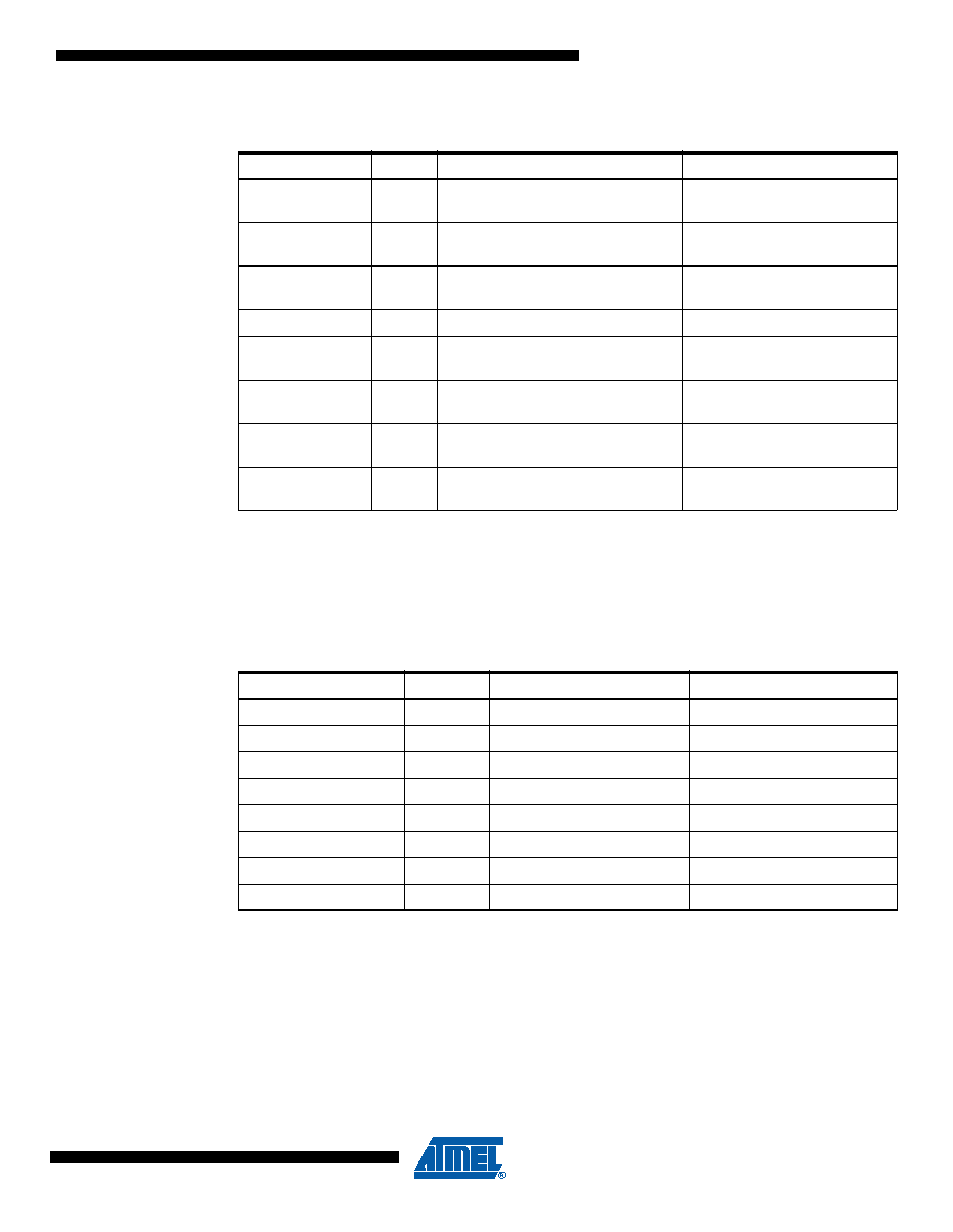
Table 25-4.
Fuse High Byte
Fuse High Byte
Bit No
Description
Default Value : 0xD9
DWEN(4)
7
Enable debugWIRE (and disable
Reset capability
1 (unprogrammed, debugWIRE
disabled)
RSTDSBL
6
Disable Reset (pin can be used as
general purpose I/O)
1 (unprogrammed, Reset
enabled)
5
Enable Serial Program and Data
Downloading
0 (programmed, SPI prog.
enabled)
WDTON(3)
4
Watchdog Timer always ON
1 (unprogrammed)(3)
EESAVE
3
EEPROM memory is preserved
through the Chip Erase
1 (unprogrammed, EEPROM
not preserved)
BOOTSZ1
2
Select Boot Size (see Table 25-9 for
details)
0 (programmed)(2)
BOOTSZ0
1
Select Boot Size (see Table 25-9 for
details)
0 (programmed)(2)
BOOTRST
0
Select Bootloader Address as Reset
Vector
1 (unprogrammed, Reset
vector @0x0000)
Table 25-5.
Fuse Low Byte
Fuse Low Byte
Bit No
Description
Default Value : 0x5E
CKDIV8(4)
7
Divide clock by 8
0 (programmed)
CKOUT(3)
6
Clock output
1 (unprogrammed)
SUT1
5
Select start-up time
SUT0
4
Select start-up time
CKSEL3
3
Select Clock source
CKSEL2
2
Select Clock source
CKSEL1
1
Select Clock source
CKSEL0
0
Select Clock source
相關(guān)PDF資料 |
PDF描述 |
|---|---|
| MD83C154XXX-12/883D | 8-BIT, MROM, 12 MHz, MICROCONTROLLER, CDIP40 |
| MR83C154XXX-12P883R | 8-BIT, MROM, 12 MHz, MICROCONTROLLER, CQCC44 |
| MR83C154XXX-L16/883 | 8-BIT, MROM, 16 MHz, MICROCONTROLLER, CQCC44 |
| MC80C32E-16:D | 8-BIT, 16 MHz, MICROCONTROLLER, CDIP40 |
| MC80C32E-25 | 8-BIT, 25 MHz, MICROCONTROLLER, CDIP40 |
相關(guān)代理商/技術(shù)參數(shù) |
參數(shù)描述 |
|---|---|
| MQ82370-20 | 制造商:Rochester Electronics LLC 功能描述:- Bulk |
| MQ8238020 | 制造商:Intel 功能描述:CONTROLLER: OTHER |
| MQ82380-20 | 制造商:Rochester Electronics LLC 功能描述:- Bulk |
| MQ82380-20/R | 制造商:Rochester Electronics LLC 功能描述: |
| MQ82592 | 制造商:Rochester Electronics LLC 功能描述:- Bulk |
發(fā)布緊急采購(gòu),3分鐘左右您將得到回復(fù)。