- 您現(xiàn)在的位置:買賣IC網(wǎng) > PDF目錄369928 > MPX2000 (Motorola, Inc.) Pressure Sensor(壓力傳感器) PDF資料下載
參數(shù)資料
| 型號: | MPX2000 |
| 廠商: | Motorola, Inc. |
| 英文描述: | Pressure Sensor(壓力傳感器) |
| 中文描述: | 壓力傳感器(壓力傳感器) |
| 文件頁數(shù): | 2/6頁 |
| 文件大小: | 109K |
| 代理商: | MPX2000 |

2
Motorola Sensor Device Data
PRESSURE SENSOR CHARACTERISTICS
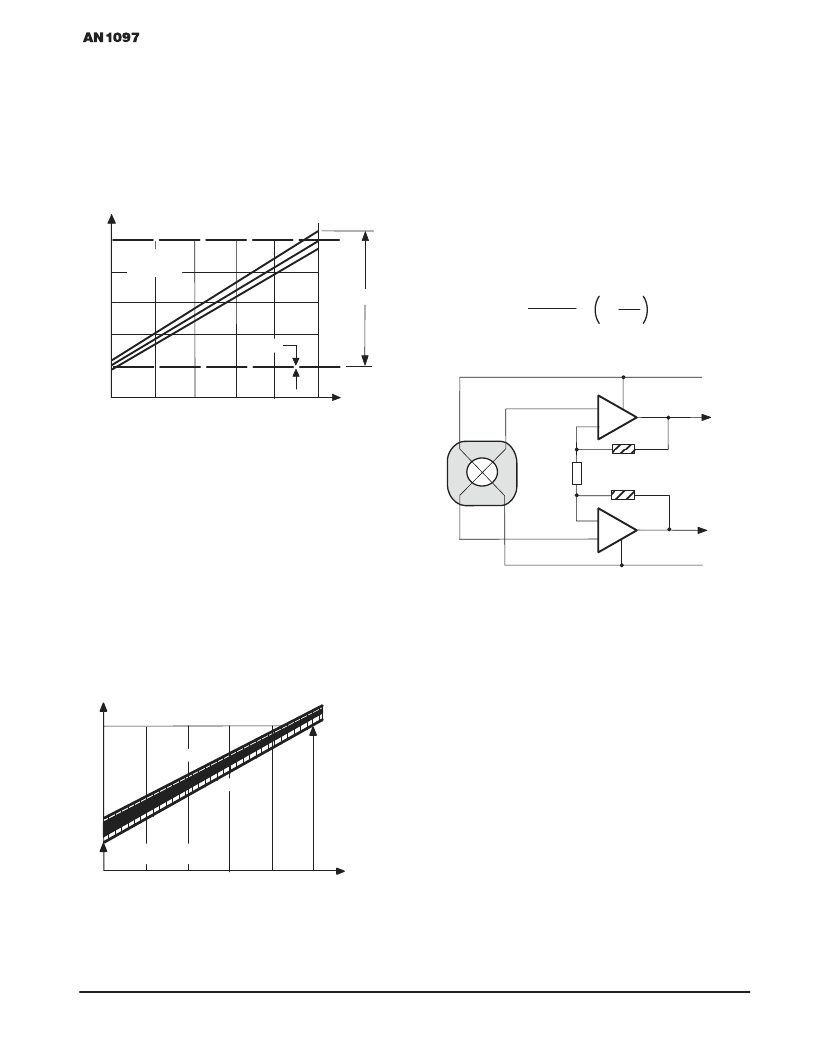
Figure 2 shows the differential output voltage of the
MPX2100 series at +25
°
C. The dispersion of the output
voltage determines the best tolerance that the system may
achieve without undertaking a calibration procedure, if any
other elements or parameters in the chain do not introduce
additional errors.
V
out
(mV)
V
S
= 5 Vdc
T
A
= 25
°
C
P
(kPa)
FULL–SCALE
20
10
5
0
–5
0
20
40
60
80
100
OFFSET
Figure 2. Spread of the Output Voltage versus the
Applied Pressure at 25
°
C
The effects of temperature on the full scale output and offset
are shown in Figure 3. It is interesting to notice that the offset
variation is greater than the full scale output and both have a
positive temperature coefficient respectively of +8.0
μ
V/degree and +5.0
μ
V excitation voltage. That means that
the full scale variation may be compensated by modifying the
gain somewhere in the chain amplifier by components
arranged to produce a negative T
C
of 250 PPM/
°
C. The dark
area of Figure 3 shows the trend of the compensation which
improves the full scale value over the temperature range. In
the area of 40 kPa, the compensation acts in the ratio of
40/100 of the value of the offset temperature coefficient.
Figure 3. Output Voltage versus Temperature. The
Dark Area Shows the Trend of the Compensation
V
out
(f)
T
POSITIVE
FULL SCALE
VARIATION
P
(kPa)
0
20
40
60
80
100
OFFSET VARIATION
–15
°
C
+85
°
C
OP AMP CHARACTERISTICS
For systems with only one power supply, the instrument
amplifier configuration shown in Figure 4 is a good solution to
monitor the output of a resistive transducer bridge.
The instrument amplifier does provide an excellent CMRR
and a symmetrical buffered high input impedance at both
non–inverting and inverting terminals. It minimizes the
number of the external passive components used to set the
gain of the amplifier. Also, it is easy to compensate the
temperature variation of the Full Scale Output of the Pressure
Sensor by implementing resistors “R
f
” having a negative
coefficient temperature of –250 PPM/
°
C.
The differential–mode voltage gain of the instrument
amplifier is:
Avd =
V1–V2
1 +2 R
f
R
g
(1)
+V
s
V1
V2
0 V
–
+
R
f
g
2
4
Figure 4. One Power Supply to Excite the Bridge
and to Develop a Differential Output Voltage
éé
éé
ééé
ééé
éé
éé
3
1
–
+
The major source of errors introduced by the op amp is
offset voltages which may be positive or negative, and the
input bias current which develops a drop voltage
V through
the feedback resistance R
f
. When the op amp input is
composed of PNP transistors, the whole characteristic of the
transfer function is shifted below the DC component voltage
value set by the Pressure Sensor as shown in Figure 5.
The gain of the instrument amplifier is calculated carefully
to avoid a saturation of the output voltage, and to provide the
maximum of differential output voltage available for the A/D
Converter. The maximum output swing voltage of the
amplifiers is also dependent on the bias current which creates
a
V voltage on the feedback resistance R
f
and on the Full
Scale output voltage of the pressure sensor.
相關(guān)PDF資料 |
PDF描述 |
|---|---|
| MPX2010 | Pressure Sensor(壓力傳感器) |
| MPX2053 | 50 KPA ON CHIP TEMPERATURE COMPENSATED CALIBRATED SILICON PRESSURE SENSORS |
| MPXV2053DP | 50 KPA ON CHIP TEMPERATURE COMPENSATED CALIBRATED SILICON PRESSURE SENSORS |
| MPXV2053G | 50 KPA ON CHIP TEMPERATURE COMPENSATED CALIBRATED SILICON PRESSURE SENSORS |
| MPXV2053GP | 50 KPA ON CHIP TEMPERATURE COMPENSATED CALIBRATED SILICON PRESSURE SENSORS |
相關(guān)代理商/技術(shù)參數(shù) |
參數(shù)描述 |
|---|---|
| MPX200A | 制造商:MOTOROLA 制造商全稱:Motorola, Inc 功能描述:0 to 200 kPa (0-29 psi) 60 mV FULL SCALE SPAN (TYPICAL) |
| MPX200AP | 制造商:MOTOROLA 制造商全稱:Motorola, Inc 功能描述:0 to 200 kPa (0-29 psi) 60 mV FULL SCALE SPAN (TYPICAL) |
| MPX200AS | 制造商:MOTOROLA 制造商全稱:Motorola, Inc 功能描述:0 to 200 kPa (0-29 psi) 60 mV FULL SCALE SPAN (TYPICAL) |
| MPX200ASX | 制造商:MOTOROLA 制造商全稱:Motorola, Inc 功能描述:0 to 200 kPa (0-29 psi) 60 mV FULL SCALE SPAN (TYPICAL) |
| MPX200D | 制造商:MOTOROLA 制造商全稱:Motorola, Inc 功能描述:X-ducer SILICON PRESSURE SENSOR |
發(fā)布緊急采購,3分鐘左右您將得到回復(fù)。