- 您現(xiàn)在的位置:買賣IC網(wǎng) > PDF目錄69037 > MPC9850VFR2 (FREESCALE SEMICONDUCTOR INC) 500 MHz, PROC SPECIFIC CLOCK GENERATOR, PBGA100 PDF資料下載
參數(shù)資料
| 型號: | MPC9850VFR2 |
| 廠商: | FREESCALE SEMICONDUCTOR INC |
| 元件分類: | 時鐘產(chǎn)生/分配 |
| 英文描述: | 500 MHz, PROC SPECIFIC CLOCK GENERATOR, PBGA100 |
| 封裝: | MAPBGA-100 |
| 文件頁數(shù): | 7/12頁 |
| 文件大小: | 243K |
| 代理商: | MPC9850VFR2 |
Advanced Clock Drivers Devices
4
Freescale Semiconductor
MPC9850
OPERATION INFORMATION
Output Frequency Configuration
The MPC9850 was designed to provide the commonly
used frequencies in PowerQUICC, PowerPC and other
microprocessor systems. Table 3 lists the configuration
values that will generate those common frequencies. The
MPC9850 can generate numerous other frequencies that
may be useful in specific applications. The output frequency
(fout) of either Bank A or Bank B may be calculated by the
following equation.
fout = 2000 / N
where fout is in MHz and N = 2 * CLK_x[0:5]
This calculation is valid for all values of N from 8 to 126.
Note that N = 15 is a modified case of the configuration inputs
CLK_x[0:5]. To achieve N = 15 CLK_x[0:5] is configured to
00111 or 7.
Crystal Input Operation
TBD
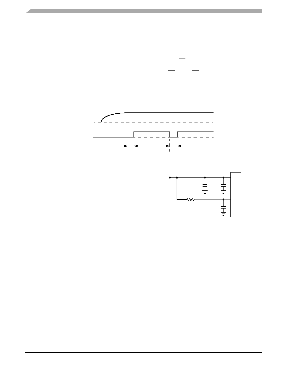
Power-Up and MR Operation
Figure 2 defines the release time and the minimum pulse
length for MR pin. The MR release time is based upon the
power supply being stable and within VDD specifications. See
Table 11 for actual parameter values. The MPC9850 may be
configured after release of reset and the outputs will be stable
for use after lock indication is obtained.
Figure 2. MR Operation
Power Supply Bypassing
The MPC9850 is a mixed analog/digital product. The
architecture of the MPC9850 supports low noise signal
operation at high frequencies. In order to maintain its superior
signal quality, all VDD pins should be bypassed by
high-frequency ceramic capacitors connected to GND. If the
spectral frequencies of the internally generated switching
noise on the supply pins cross the series resonant point of an
individual bypass capacitor, its overall impedance begins to
look inductive and thus increases with increasing frequency.
The parallel capacitor combination shown ensures that a low
impedance path to ground exists for frequencies well above
the noise bandwidth.
Figure 3. VCC Power Supply Bypass
MR
VDD
treset_rel
treset_pulse
VDD
MPC9850
0.1
F
22
F
0.1
F
15
VDD
VDDA
相關(guān)PDF資料 |
PDF描述 |
|---|---|
| MPC9992FAR2 | 400 MHz, OTHER CLOCK GENERATOR, PQFP32 |
| MPD70F3224GC(A)-8EU | RISC MICROCONTROLLER, PQFP100 |
| MPD70F3226GC(A)-8EU | RISC MICROCONTROLLER, PQFP100 |
| MPD800261F1-523-HN2 | 32-BIT, 150 MHz, RISC MICROCONTROLLER, PBGA304 |
| MPD800261F1-523-HN2 | 32-BIT, 150 MHz, RISC MICROCONTROLLER, PBGA304 |
相關(guān)代理商/技術(shù)參數(shù) |
參數(shù)描述 |
|---|---|
| MPC9850VM | 功能描述:時鐘發(fā)生器及支持產(chǎn)品 RoHS:否 制造商:Silicon Labs 類型:Clock Generators 最大輸入頻率:14.318 MHz 最大輸出頻率:166 MHz 輸出端數(shù)量:16 占空比 - 最大:55 % 工作電源電壓:3.3 V 工作電源電流:1 mA 最大工作溫度:+ 85 C 安裝風(fēng)格:SMD/SMT 封裝 / 箱體:QFN-56 |
| MPC9850VMR2 | 功能描述:時鐘發(fā)生器及支持產(chǎn)品 RoHS:否 制造商:Silicon Labs 類型:Clock Generators 最大輸入頻率:14.318 MHz 最大輸出頻率:166 MHz 輸出端數(shù)量:16 占空比 - 最大:55 % 工作電源電壓:3.3 V 工作電源電流:1 mA 最大工作溫度:+ 85 C 安裝風(fēng)格:SMD/SMT 封裝 / 箱體:QFN-56 |
| MPC9855 | 制造商:MOTOROLA 制造商全稱:Motorola, Inc 功能描述:Clock Generator for PowerQUICC and PowerPC Microprocessors |
| MPC9855VM | 功能描述:時鐘發(fā)生器及支持產(chǎn)品 RoHS:否 制造商:Silicon Labs 類型:Clock Generators 最大輸入頻率:14.318 MHz 最大輸出頻率:166 MHz 輸出端數(shù)量:16 占空比 - 最大:55 % 工作電源電壓:3.3 V 工作電源電流:1 mA 最大工作溫度:+ 85 C 安裝風(fēng)格:SMD/SMT 封裝 / 箱體:QFN-56 |
| MPC9855VMR2 | 功能描述:時鐘發(fā)生器及支持產(chǎn)品 RoHS:否 制造商:Silicon Labs 類型:Clock Generators 最大輸入頻率:14.318 MHz 最大輸出頻率:166 MHz 輸出端數(shù)量:16 占空比 - 最大:55 % 工作電源電壓:3.3 V 工作電源電流:1 mA 最大工作溫度:+ 85 C 安裝風(fēng)格:SMD/SMT 封裝 / 箱體:QFN-56 |
發(fā)布緊急采購,3分鐘左右您將得到回復(fù)。