- 您現(xiàn)在的位置:買賣IC網(wǎng) > PDF目錄25631 > MPC8548VTAVJB (FREESCALE SEMICONDUCTOR INC) 32-BIT, 1500 MHz, MICROPROCESSOR, PBGA783 PDF資料下載
參數(shù)資料
| 型號: | MPC8548VTAVJB |
| 廠商: | FREESCALE SEMICONDUCTOR INC |
| 元件分類: | 微控制器/微處理器 |
| 英文描述: | 32-BIT, 1500 MHz, MICROPROCESSOR, PBGA783 |
| 封裝: | 29 X 29 MM, 1 MM PITCH, FLIP CHIP, LEAD FREE, PLASTIC, BGA-783 |
| 文件頁數(shù): | 94/142頁 |
| 文件大小: | 1504K |
| 代理商: | MPC8548VTAVJB |
第1頁第2頁第3頁第4頁第5頁第6頁第7頁第8頁第9頁第10頁第11頁第12頁第13頁第14頁第15頁第16頁第17頁第18頁第19頁第20頁第21頁第22頁第23頁第24頁第25頁第26頁第27頁第28頁第29頁第30頁第31頁第32頁第33頁第34頁第35頁第36頁第37頁第38頁第39頁第40頁第41頁第42頁第43頁第44頁第45頁第46頁第47頁第48頁第49頁第50頁第51頁第52頁第53頁第54頁第55頁第56頁第57頁第58頁第59頁第60頁第61頁第62頁第63頁第64頁第65頁第66頁第67頁第68頁第69頁第70頁第71頁第72頁第73頁第74頁第75頁第76頁第77頁第78頁第79頁第80頁第81頁第82頁第83頁第84頁第85頁第86頁第87頁第88頁第89頁第90頁第91頁第92頁第93頁當前第94頁第95頁第96頁第97頁第98頁第99頁第100頁第101頁第102頁第103頁第104頁第105頁第106頁第107頁第108頁第109頁第110頁第111頁第112頁第113頁第114頁第115頁第116頁第117頁第118頁第119頁第120頁第121頁第122頁第123頁第124頁第125頁第126頁第127頁第128頁第129頁第130頁第131頁第132頁第133頁第134頁第135頁第136頁第137頁第138頁第139頁第140頁第141頁第142頁
MPC8548E PowerQUICC III Integrated Processor Hardware Specifications, Rev. 5
Freescale Semiconductor
55
I
2C
13.2
I2C AC Electrical Specifications
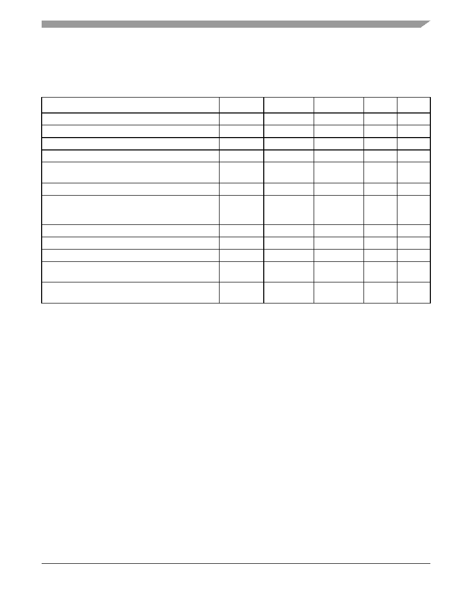
Table 46. I2C AC Electrical Specifications
Parameter
Symbol1
Min
Max
Unit
Notes
SCL clock frequency
fI2C
0400
kHz
—
Low period of the SCL clock
tI2CL
1.3
—
μs4
High period of the SCL clock
tI2CH
0.6
—
μs4
Setup time for a repeated START condition
tI2SVKH
0.6
—
μs4
Hold time (repeated) START condition (after this period,
the first clock pulse is generated)
tI2SXKL
0.6
—
μs4
Data setup time
tI2DVKH
100
—
ns
4
Data input hold time:
CBUS compatible masters
I2C bus devices
tI2DXKL
—
0
—
μs2
Data output delay time:
tI2OVKL
—0.9
—
3
Set-up time for STOP condition
tI2PVKH
0.6
—
μs—
Bus free time between a STOP and START condition
tI2KHDX
1.3
—
μs—
Noise margin at the LOW level for each connected device
(including hysteresis)
VNL
0.1
× OVDD
—V
—
Noise margin at the HIGH level for each connected
device (including hysteresis)
VNH
0.2
× OVDD
—V
—
Notes:
1. The symbols used for timing specifications follow the pattern of t(first two letters of functional block)(signal)(state)(reference)(state) for
inputs and t(first two letters of functional block)(reference)(state)(signal)(state) for outputs. For example, tI2DVKH symbolizes I
2C timing (I2)
with respect to the time data input signals (D) reach the valid state (V) relative to the tI2C clock reference (K) going to the high
(H) state or setup time. Also, tI2SXKL symbolizes I
2C timing (I2) for the time that the data with respect to the start condition
(S) went invalid (X) relative to the tI2C clock reference (K) going to the low (L) state or hold time. Also, tI2PVKH symbolizes I
2C
timing (I2) for the time that the data with respect to the stop condition (P) reaching the valid state (V) relative to the tI2C clock
reference (K) going to the high (H) state or setup time. For rise and fall times, the latter convention is used with the appropriate
letter: R (rise) or F (fall).
2. As a transmitter, the MPC8548E provides a delay time of at least 300 ns for the SDA signal (refer to the VIH(min) of the SCL
signal) to bridge the undefined region of the falling edge of SCL to avoid unintended generation of Start or Stop condition.
When MPC8548E acts as the I2C bus master while transmitting, MPC8548E drives both SCL and SDA. As long as the load
on SCL and SDA are balanced, MPC8548E would not cause unintended generation of Start or Stop condition. Therefore,
the 300 ns SDA output delay time is not a concern. If, under some rare condition, the 300 ns SDA output delay time is required
for MPC8548E as transmitter, the following setting is recommended for the FDR bit field of the I2CFDR register to ensure
both the desired I2C SCL clock frequency and SDA output delay time are achieved, assuming that the desired I2C SCL clock
frequency is 400 kHz and the Digital Filter Sampling Rate Register (I2CDFSRR) is programmed with its default setting of
0x10 (decimal 16):
I2C source clock frequency
333 MHz
266 MHz
200 MHz
133 MHz
FDR bit setting
0x2A
0x05
0x26
0x00
Actual FDR divider selected
896
704
512
384
Actual I2C SCL frequency generated
371 kHz
378 kHz
390 kHz
346 kHz
For the detail of I2C frequency calculation, refer to Freescale Application Note AN2919,
Determining the I2C Frequency
Divider Ratio for SCL. Note that the I2C source clock frequency is half of the CCB clock frequency for MPC8548E.
3. The maximum tI2DXKL has only to be met if the device does not stretch the LOW period (tI2CL) of the SCL signal.
4. Guaranteed by design.
相關PDF資料 |
PDF描述 |
|---|---|
| MPC8555CPXALF | 32-BIT, 667 MHz, RISC PROCESSOR, PBGA783 |
| MPC8555VTALD | 32-BIT, 667 MHz, RISC PROCESSOR, PBGA783 |
| MPC8555CVTALF | 32-BIT, 667 MHz, RISC PROCESSOR, PBGA783 |
| MPC8555EVTALD | 32-BIT, 667 MHz, RISC PROCESSOR, PBGA783 |
| MPC8555ECPXAJF | RISC PROCESSOR, PBGA783 |
相關代理商/技術參數(shù) |
參數(shù)描述 |
|---|---|
| MPC8548VUAQG | 功能描述:微處理器 - MPU PQ38 8548 PB-FREE RoHS:否 制造商:Atmel 處理器系列:SAMA5D31 核心:ARM Cortex A5 數(shù)據(jù)總線寬度:32 bit 最大時鐘頻率:536 MHz 程序存儲器大小:32 KB 數(shù)據(jù) RAM 大小:128 KB 接口類型:CAN, Ethernet, LIN, SPI,TWI, UART, USB 工作電源電壓:1.8 V to 3.3 V 最大工作溫度:+ 85 C 安裝風格:SMD/SMT 封裝 / 箱體:FBGA-324 |
| MPC8548VUATG | 功能描述:微處理器 - MPU PQ38 8548 PB-FREE RoHS:否 制造商:Atmel 處理器系列:SAMA5D31 核心:ARM Cortex A5 數(shù)據(jù)總線寬度:32 bit 最大時鐘頻率:536 MHz 程序存儲器大小:32 KB 數(shù)據(jù) RAM 大小:128 KB 接口類型:CAN, Ethernet, LIN, SPI,TWI, UART, USB 工作電源電壓:1.8 V to 3.3 V 最大工作溫度:+ 85 C 安裝風格:SMD/SMT 封裝 / 箱體:FBGA-324 |
| MPC8548VUAUJ | 功能描述:微處理器 - MPU PQ38 8548 PB-FREE RoHS:否 制造商:Atmel 處理器系列:SAMA5D31 核心:ARM Cortex A5 數(shù)據(jù)總線寬度:32 bit 最大時鐘頻率:536 MHz 程序存儲器大小:32 KB 數(shù)據(jù) RAM 大小:128 KB 接口類型:CAN, Ethernet, LIN, SPI,TWI, UART, USB 工作電源電壓:1.8 V to 3.3 V 最大工作溫度:+ 85 C 安裝風格:SMD/SMT 封裝 / 箱體:FBGA-324 |
| MPC8548VUAVH | 制造商:Freescale Semiconductor 功能描述:MPU RISC 32BIT CMOS 1.5GHZ 1.8V/2.5V/3.3V 783FCCBGA - Bulk |
| MPC8548VUAVK | 制造商:Freescale Semiconductor 功能描述:PQ38 8548 PB-FREE - Bulk |
發(fā)布緊急采購,3分鐘左右您將得到回復。