- 您現(xiàn)在的位置:買賣IC網(wǎng) > PDF目錄45366 > MPC8535ECVTAKG (FREESCALE SEMICONDUCTOR INC) 32-BIT, 600 MHz, MICROPROCESSOR, PBGA783 PDF資料下載
參數(shù)資料
| 型號: | MPC8535ECVTAKG |
| 廠商: | FREESCALE SEMICONDUCTOR INC |
| 元件分類: | 微控制器/微處理器 |
| 英文描述: | 32-BIT, 600 MHz, MICROPROCESSOR, PBGA783 |
| 封裝: | 29 X 29 MM, 2.80 MM HEIGHT, 1 MM PITCH, LEAD FREE, PLASTIC, FCBGA-783 |
| 文件頁數(shù): | 62/126頁 |
| 文件大小: | 2861K |
| 代理商: | MPC8535ECVTAKG |
第1頁第2頁第3頁第4頁第5頁第6頁第7頁第8頁第9頁第10頁第11頁第12頁第13頁第14頁第15頁第16頁第17頁第18頁第19頁第20頁第21頁第22頁第23頁第24頁第25頁第26頁第27頁第28頁第29頁第30頁第31頁第32頁第33頁第34頁第35頁第36頁第37頁第38頁第39頁第40頁第41頁第42頁第43頁第44頁第45頁第46頁第47頁第48頁第49頁第50頁第51頁第52頁第53頁第54頁第55頁第56頁第57頁第58頁第59頁第60頁第61頁當前第62頁第63頁第64頁第65頁第66頁第67頁第68頁第69頁第70頁第71頁第72頁第73頁第74頁第75頁第76頁第77頁第78頁第79頁第80頁第81頁第82頁第83頁第84頁第85頁第86頁第87頁第88頁第89頁第90頁第91頁第92頁第93頁第94頁第95頁第96頁第97頁第98頁第99頁第100頁第101頁第102頁第103頁第104頁第105頁第106頁第107頁第108頁第109頁第110頁第111頁第112頁第113頁第114頁第115頁第116頁第117頁第118頁第119頁第120頁第121頁第122頁第123頁第124頁第125頁第126頁
MPC8535E PowerQUICC III Integrated Processor Hardware Specifications, Rev. 3
Ethernet: Enhanced Three-Speed Ethernet (eTSEC), MII Management
Freescale Semiconductor
40
2.9.1
Enhanced Three-Speed Ethernet Controller (eTSEC)
(10/100/1000 Mbps) — FIFO/GMII/MII/TBI/RGMII/RTBI/RMII Electrical
Characteristics
The electrical characteristics specified here apply to all FIFO mode, gigabit media independent interface (GMII), media
independent interface (MII), ten-bit interface (TBI), reduced gigabit media independent interface (RGMII), reduced ten-bit
interface (RTBI), and reduced media independent interface (RMII) signals except management data input/output (MDIO) and
management data clock (MDC), and serial gigabit media independent interface (SGMII). The RGMII, RTBI and FIFO mode
interfaces are defined for 2.5 V, while the GMII, MII, RMII, and TBI interfaces can operate at 3.3V.
The GMII, MII, or TBI interface timing is compliant with IEEE 802.3. The RGMII and RTBI interfaces follow the Reduced
Gigabit Media-Independent Interface (RGMII) Specification Version 1.3 (12/10/2000). The RMII interface follows the RMII
Consortium RMII Specification Version 1.2 (3/20/1998).
The electrical characteristics for MDIO and MDC are specified in Section 2.10, “Ethernet Management Interface Electrical
The electrical characteristics for SGMII is specified in Section 2.9.3, “SGMII Interface Electrical Characteristics.” The SGMII
interface conforms (with exceptions) to the Serial-GMII Specification Version 1.8.
2.9.1.1
GMII, MII, TBI, RGMII, RMII and RTBI DC Electrical Characteristics
All GMII, MII, TBI, RGMII, RMII and RTBI drivers and receivers comply with the DC parametric attributes specified in
Table 24 and Table 25. The RGMII and RTBI signals are based on a 2.5-V CMOS interface voltage as defined by JEDEC
EIA/JESD8-5.
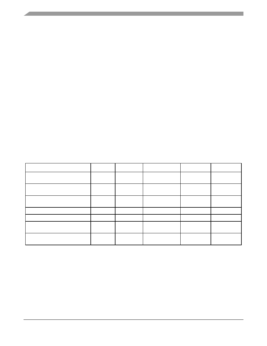
Table 24. GMII, MII, RMII, and TBI DC Electrical Characteristics
Parameter
Symbol
Min
Max
Unit
Notes
Supply voltage 3.3 V
LVDD
TVDD
3.13
3.47
V
1, 2
1 LV
DD supports eTSECs 1.
2 TV
DD supports eTSECs 3.
Output high voltage
(LVDD/TVDD = Min, IOH = –4.0 mA)
VOH
2.40
LVDD/TVDD + 0.3
V
—
Output low voltage
(LVDD/TVDD = Min, IOL = 4.0 mA)
VOL
GND
0.50
V
—
Input high voltage
VIH
1.90
LVDD/TVDD + 0.3
V
—
Input low voltage
VIL
–0.3
0.90
V
—
Input high current
(VIN = LVDD, VIN = TVDD)
IIH
—40
μA
1, 2,3
3 The symbol V
IN, in this case, represents the LVIN and TVIN symbols referenced in Table 1 and Table 2.
Input low current
(VIN = GND)
IIL
–600
—
μA
3
Notes:
發(fā)布緊急采購,3分鐘左右您將得到回復。