- 您現(xiàn)在的位置:買賣IC網(wǎng) > PDF目錄45366 > MPC8535EBVTAKGA (FREESCALE SEMICONDUCTOR INC) 32-BIT, 600 MHz, MICROPROCESSOR, PBGA783 PDF資料下載
參數(shù)資料
| 型號: | MPC8535EBVTAKGA |
| 廠商: | FREESCALE SEMICONDUCTOR INC |
| 元件分類: | 微控制器/微處理器 |
| 英文描述: | 32-BIT, 600 MHz, MICROPROCESSOR, PBGA783 |
| 封裝: | 29 X 29 MM, 2.80 MM HEIGHT, 1 MM PITCH, LEAD FREE, PLASTIC, FCBGA-783 |
| 文件頁數(shù): | 57/126頁 |
| 文件大小: | 2861K |
| 代理商: | MPC8535EBVTAKGA |
第1頁第2頁第3頁第4頁第5頁第6頁第7頁第8頁第9頁第10頁第11頁第12頁第13頁第14頁第15頁第16頁第17頁第18頁第19頁第20頁第21頁第22頁第23頁第24頁第25頁第26頁第27頁第28頁第29頁第30頁第31頁第32頁第33頁第34頁第35頁第36頁第37頁第38頁第39頁第40頁第41頁第42頁第43頁第44頁第45頁第46頁第47頁第48頁第49頁第50頁第51頁第52頁第53頁第54頁第55頁第56頁當(dāng)前第57頁第58頁第59頁第60頁第61頁第62頁第63頁第64頁第65頁第66頁第67頁第68頁第69頁第70頁第71頁第72頁第73頁第74頁第75頁第76頁第77頁第78頁第79頁第80頁第81頁第82頁第83頁第84頁第85頁第86頁第87頁第88頁第89頁第90頁第91頁第92頁第93頁第94頁第95頁第96頁第97頁第98頁第99頁第100頁第101頁第102頁第103頁第104頁第105頁第106頁第107頁第108頁第109頁第110頁第111頁第112頁第113頁第114頁第115頁第116頁第117頁第118頁第119頁第120頁第121頁第122頁第123頁第124頁第125頁第126頁
MPC8535E PowerQUICC III Integrated Processor Hardware Specifications, Rev. 3
DDR2 and DDR3 SDRAM
Freescale Semiconductor
36
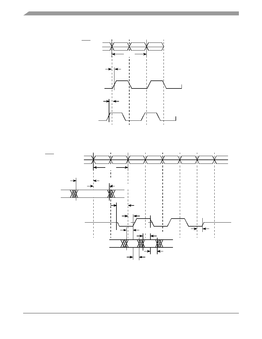
Figure 9. Timing Diagram for tDDKHMH
Figure 10 shows the DDR SDRAM output timing diagram.
Figure 10. DDR SDRAM Output Timing Diagram
MDQS
MCK[n]
tMCK
tDDKHMHmax) = 0.6 ns
tDDKHMH(min) = –0.6 ns
MDQS
ADDR/CMD
tDDKHAS ,tDDKHCS
tDDKHMH
tDDKLDS
tDDKHDS
MDQ[x]
MDQS[n]
MCK[n]
tMCK
tDDKLDX
tDDKHDX
D1
D0
tDDKHAX ,tDDKHCX
Write A0
NOOP
tDDKHME
tDDKHMP
相關(guān)PDF資料 |
PDF描述 |
|---|---|
| MPC8535CVTANGA | 32-BIT, 800 MHz, MICROPROCESSOR, PBGA783 |
| MPC8535ECVTATH | 32-BIT, 1250 MHz, MICROPROCESSOR, PBGA783 |
| MPC8535ECVTATHA | 32-BIT, 1250 MHz, MICROPROCESSOR, PBGA783 |
| MPC8535AVTATHA | 32-BIT, 1250 MHz, MICROPROCESSOR, PBGA783 |
| MPC8535CVTAQG | 32-BIT, 1000 MHz, MICROPROCESSOR, PBGA783 |
相關(guān)代理商/技術(shù)參數(shù) |
參數(shù)描述 |
|---|---|
| MPC8535EBVTANG | 功能描述:微處理器 - MPU 8535E INDUSTRIAL 800 RoHS:否 制造商:Atmel 處理器系列:SAMA5D31 核心:ARM Cortex A5 數(shù)據(jù)總線寬度:32 bit 最大時鐘頻率:536 MHz 程序存儲器大小:32 KB 數(shù)據(jù) RAM 大小:128 KB 接口類型:CAN, Ethernet, LIN, SPI,TWI, UART, USB 工作電源電壓:1.8 V to 3.3 V 最大工作溫度:+ 85 C 安裝風(fēng)格:SMD/SMT 封裝 / 箱體:FBGA-324 |
| MPC8535EBVTANGA | 功能描述:微處理器 - MPU 8535 Encrypted RoHS:否 制造商:Atmel 處理器系列:SAMA5D31 核心:ARM Cortex A5 數(shù)據(jù)總線寬度:32 bit 最大時鐘頻率:536 MHz 程序存儲器大小:32 KB 數(shù)據(jù) RAM 大小:128 KB 接口類型:CAN, Ethernet, LIN, SPI,TWI, UART, USB 工作電源電壓:1.8 V to 3.3 V 最大工作溫度:+ 85 C 安裝風(fēng)格:SMD/SMT 封裝 / 箱體:FBGA-324 |
| MPC8535EBVTAQG | 功能描述:微處理器 - MPU 8535E INDUSTRIAL 1000 RoHS:否 制造商:Atmel 處理器系列:SAMA5D31 核心:ARM Cortex A5 數(shù)據(jù)總線寬度:32 bit 最大時鐘頻率:536 MHz 程序存儲器大小:32 KB 數(shù)據(jù) RAM 大小:128 KB 接口類型:CAN, Ethernet, LIN, SPI,TWI, UART, USB 工作電源電壓:1.8 V to 3.3 V 最大工作溫度:+ 85 C 安裝風(fēng)格:SMD/SMT 封裝 / 箱體:FBGA-324 |
| MPC8535EBVTAQGA | 功能描述:微處理器 - MPU 8535 Encrypted RoHS:否 制造商:Atmel 處理器系列:SAMA5D31 核心:ARM Cortex A5 數(shù)據(jù)總線寬度:32 bit 最大時鐘頻率:536 MHz 程序存儲器大小:32 KB 數(shù)據(jù) RAM 大小:128 KB 接口類型:CAN, Ethernet, LIN, SPI,TWI, UART, USB 工作電源電壓:1.8 V to 3.3 V 最大工作溫度:+ 85 C 安裝風(fēng)格:SMD/SMT 封裝 / 箱體:FBGA-324 |
| MPC8535EBVTATH | 功能描述:微處理器 - MPU 8535E INDUSTRIAL 1250 RoHS:否 制造商:Atmel 處理器系列:SAMA5D31 核心:ARM Cortex A5 數(shù)據(jù)總線寬度:32 bit 最大時鐘頻率:536 MHz 程序存儲器大小:32 KB 數(shù)據(jù) RAM 大小:128 KB 接口類型:CAN, Ethernet, LIN, SPI,TWI, UART, USB 工作電源電壓:1.8 V to 3.3 V 最大工作溫度:+ 85 C 安裝風(fēng)格:SMD/SMT 封裝 / 箱體:FBGA-324 |
發(fā)布緊急采購,3分鐘左右您將得到回復(fù)。