- 您現(xiàn)在的位置:買賣IC網(wǎng) > PDF目錄45361 > MPC8347CVRAJFB (FREESCALE SEMICONDUCTOR INC) 32-BIT, 533 MHz, MICROPROCESSOR, PBGA620 PDF資料下載
參數(shù)資料
| 型號: | MPC8347CVRAJFB |
| 廠商: | FREESCALE SEMICONDUCTOR INC |
| 元件分類: | 微控制器/微處理器 |
| 英文描述: | 32-BIT, 533 MHz, MICROPROCESSOR, PBGA620 |
| 封裝: | 29 X 29 MM, 2.46 MM HEIGHT, 1 MM PITCH, LEAD FREE, PLASTIC, BGA-620 |
| 文件頁數(shù): | 73/98頁 |
| 文件大小: | 1084K |
| 代理商: | MPC8347CVRAJFB |
第1頁第2頁第3頁第4頁第5頁第6頁第7頁第8頁第9頁第10頁第11頁第12頁第13頁第14頁第15頁第16頁第17頁第18頁第19頁第20頁第21頁第22頁第23頁第24頁第25頁第26頁第27頁第28頁第29頁第30頁第31頁第32頁第33頁第34頁第35頁第36頁第37頁第38頁第39頁第40頁第41頁第42頁第43頁第44頁第45頁第46頁第47頁第48頁第49頁第50頁第51頁第52頁第53頁第54頁第55頁第56頁第57頁第58頁第59頁第60頁第61頁第62頁第63頁第64頁第65頁第66頁第67頁第68頁第69頁第70頁第71頁第72頁當(dāng)前第73頁第74頁第75頁第76頁第77頁第78頁第79頁第80頁第81頁第82頁第83頁第84頁第85頁第86頁第87頁第88頁第89頁第90頁第91頁第92頁第93頁第94頁第95頁第96頁第97頁第98頁
MPC8347EA PowerQUICC II Pro Integrated Host Processor Hardware Specifications, Rev. 11
Freescale Semiconductor
75
Clocking
19 Clocking
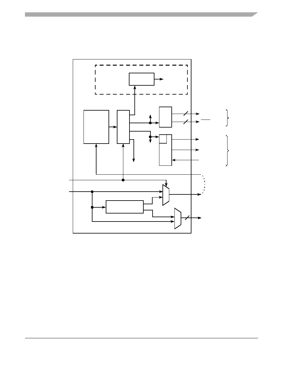
Figure 41 shows the internal distribution of the clocks.
Figure 41. MPC8347EA Clock Subsystem
The primary clock source can be one of two inputs, CLKIN or PCI_CLK, depending on whether the device
is configured in PCI host or PCI agent mode. When the MPC8347EA is configured as a PCI host device,
CLKIN is its primary input clock. CLKIN feeds the PCI clock divider (
÷2) and the multiplexors for
PCI_SYNC_OUT and PCI_CLK_OUT. The CFG_CLKIN_DIV configuration input selects whether
CLKIN or CLKIN/2 is driven out on the PCI_SYNC_OUT signal. The OCCR[PCICDn] parameters select
whether CLKIN or CLKIN/2 is driven out on the PCI_CLK_OUTn signals.
PCI_SYNC_OUT is connected externally to PCI_SYNC_IN to allow the internal clock subsystem to
synchronize to the system PCI clocks. PCI_SYNC_OUT must be connected properly to PCI_SYNC_IN,
with equal delay to all PCI agent devices in the system, to allow the MPC8347EA to function. When the
device is configured as a PCI agent device, PCI_CLK is the primary input clock and the CLKIN signal
should be tied to GND.
Core PLL
System PLL
DDR
LBIU
LSYNC_IN
LSYNC_OUT
LCLK[0:2]
MCK[0:5]
core_clk
e300 Core
csb_clk to Rest
CLKIN
csb_clk
6
DDR
Memory
Local Bus
PCI_CLK_OUT[0:4]
PCI_SYNC_OUT
PCI_CLK/
Clock
Unit
of the Device
ddr_clk
lbiu_clk
CFG_CLKIN_DIV
PCI Clock
PCI_SYNC_IN
Device
Memory
Device
/n
To Local Bus
Memory
Controller
To DDR
Memory
Controller
DLL
Clock
Div
/2
Divider
5
發(fā)布緊急采購,3分鐘左右您將得到回復(fù)。