- 您現(xiàn)在的位置:買賣IC網(wǎng) > PDF目錄45341 > MPC5604PEF0MLL4 (FREESCALE SEMICONDUCTOR INC) 32-BIT, FLASH, 40 MHz, MICROCONTROLLER, PQFP100 PDF資料下載
參數(shù)資料
| 型號(hào): | MPC5604PEF0MLL4 |
| 廠商: | FREESCALE SEMICONDUCTOR INC |
| 元件分類: | 微控制器/微處理器 |
| 英文描述: | 32-BIT, FLASH, 40 MHz, MICROCONTROLLER, PQFP100 |
| 封裝: | 14 X 14 MM, 1.40 MM HEIGHT, 0.50 MM PITCH, ROHS COMPLIANT LQFP-100 |
| 文件頁(yè)數(shù): | 70/99頁(yè) |
| 文件大小: | 1130K |
| 代理商: | MPC5604PEF0MLL4 |
第1頁(yè)第2頁(yè)第3頁(yè)第4頁(yè)第5頁(yè)第6頁(yè)第7頁(yè)第8頁(yè)第9頁(yè)第10頁(yè)第11頁(yè)第12頁(yè)第13頁(yè)第14頁(yè)第15頁(yè)第16頁(yè)第17頁(yè)第18頁(yè)第19頁(yè)第20頁(yè)第21頁(yè)第22頁(yè)第23頁(yè)第24頁(yè)第25頁(yè)第26頁(yè)第27頁(yè)第28頁(yè)第29頁(yè)第30頁(yè)第31頁(yè)第32頁(yè)第33頁(yè)第34頁(yè)第35頁(yè)第36頁(yè)第37頁(yè)第38頁(yè)第39頁(yè)第40頁(yè)第41頁(yè)第42頁(yè)第43頁(yè)第44頁(yè)第45頁(yè)第46頁(yè)第47頁(yè)第48頁(yè)第49頁(yè)第50頁(yè)第51頁(yè)第52頁(yè)第53頁(yè)第54頁(yè)第55頁(yè)第56頁(yè)第57頁(yè)第58頁(yè)第59頁(yè)第60頁(yè)第61頁(yè)第62頁(yè)第63頁(yè)第64頁(yè)第65頁(yè)第66頁(yè)第67頁(yè)第68頁(yè)第69頁(yè)當(dāng)前第70頁(yè)第71頁(yè)第72頁(yè)第73頁(yè)第74頁(yè)第75頁(yè)第76頁(yè)第77頁(yè)第78頁(yè)第79頁(yè)第80頁(yè)第81頁(yè)第82頁(yè)第83頁(yè)第84頁(yè)第85頁(yè)第86頁(yè)第87頁(yè)第88頁(yè)第89頁(yè)第90頁(yè)第91頁(yè)第92頁(yè)第93頁(yè)第94頁(yè)第95頁(yè)第96頁(yè)第97頁(yè)第98頁(yè)第99頁(yè)
MPC5604P Microcontroller Data Sheet, Rev. 7
Freescale Semiconductor
72
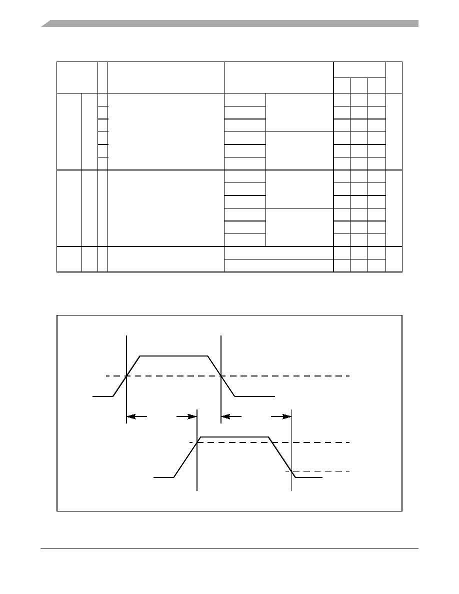
Figure 18. Pad output delay
ttr
CC D Output transition time output pin2
MEDIUM configuration
CL = 25 pF
VDD = 5.0 V ± 10%,
PAD3V5V = 0
SIUL.PCRx.SRC = 1
——
10
ns
TCL = 50 pF
—
20
DCL = 100 pF
—
40
DCL = 25 pF
VDD = 3.3 V ± 10%,
PAD3V5V = 1
SIUL.PCRx.SRC = 1
——
12
TCL = 50 pF
—
25
DCL = 100 pF
—
40
ttr
CC D Output transition time output pin2
FAST configuration
CL = 25 pF
VDD = 5.0 V ± 10%,
PAD3V5V = 0
SIUL.PCRx.SRC = 1
——
4
ns
CL = 50 pF
—
6
CL = 100 pF
—
12
CL = 25 pF
VDD = 3.3 V ± 10%,
PAD3V5V = 1
SIUL.PCRx.SRC = 1
——
4
CL = 50 pF
—
7
CL = 100 pF
—
12
tSYM
3
CC T Symmetric transition time, same drive
strength between N and P transistor
VDD = 5.0 V ± 10%, PAD3V5V = 0
—
4
ns
VDD = 3.3 V ± 10%, PAD3V5V = 1
—
5
1 V
DD = 3.3 V ± 10% / 5.0 V ± 10%, TA = –40 °C to TA MAX, unless otherwise specified
2 C
L includes device and package capacitances (CPKG < 5 pF).
3 Transition timing of both positive and negative slopes will differ maximum 50%
Table 34. Output pin transition times (continued)
Symbol
C
Parameter
Conditions1
Value
Unit
Min Typ Max
VDD_HV_IOx/2
VOH
VOL
Rising
Edge
Output
Delay
Falling
Edge
Output
Delay
Pad
Data Input
Pad
Output
發(fā)布緊急采購(gòu),3分鐘左右您將得到回復(fù)。