- 您現(xiàn)在的位置:買賣IC網(wǎng) > PDF目錄45341 > MPC5604BF1CLQ6 (FREESCALE SEMICONDUCTOR INC) MICROCONTROLLER, PQFP144 PDF資料下載
參數(shù)資料
| 型號: | MPC5604BF1CLQ6 |
| 廠商: | FREESCALE SEMICONDUCTOR INC |
| 元件分類: | 微控制器/微處理器 |
| 英文描述: | MICROCONTROLLER, PQFP144 |
| 封裝: | 20 X 20 MM, 1.40 MM HEIGHT, 0.50 MM PITCH, LQFP-144 |
| 文件頁數(shù): | 73/104頁 |
| 文件大小: | 953K |
| 代理商: | MPC5604BF1CLQ6 |
第1頁第2頁第3頁第4頁第5頁第6頁第7頁第8頁第9頁第10頁第11頁第12頁第13頁第14頁第15頁第16頁第17頁第18頁第19頁第20頁第21頁第22頁第23頁第24頁第25頁第26頁第27頁第28頁第29頁第30頁第31頁第32頁第33頁第34頁第35頁第36頁第37頁第38頁第39頁第40頁第41頁第42頁第43頁第44頁第45頁第46頁第47頁第48頁第49頁第50頁第51頁第52頁第53頁第54頁第55頁第56頁第57頁第58頁第59頁第60頁第61頁第62頁第63頁第64頁第65頁第66頁第67頁第68頁第69頁第70頁第71頁第72頁當(dāng)前第73頁第74頁第75頁第76頁第77頁第78頁第79頁第80頁第81頁第82頁第83頁第84頁第85頁第86頁第87頁第88頁第89頁第90頁第91頁第92頁第93頁第94頁第95頁第96頁第97頁第98頁第99頁第100頁第101頁第102頁第103頁第104頁
MPC5604B/C Microcontroller Data Sheet, Rev. 9
Electrical characteristics
Freescale Semiconductor
70
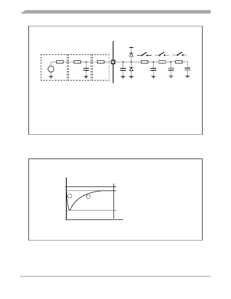
Figure 21. Input equivalent circuit (extended channels)
A second aspect involving the capacitance network shall be considered. Assuming the three capacitances CF, CP1 and CP2 are
initially charged at the source voltage VA (refer to the equivalent circuit in Figure 20): A charge sharing phenomenon is installed
when the sampling phase is started (A/D switch close).
Figure 22. Transient behavior during sampling phase
In particular two different transient periods can be distinguished:
RF
CF
RS
RL
RSW1
CP3
CS
VDD
Sampling
Source
Filter
Current Limiter
EXTERNAL CIRCUIT
INTERNAL CIRCUIT SCHEME
CP1
RAD
Channel
Selection
VA
CP2
Extended
RSW2
Switch
RS: Source impedance
RF: Filter resistance
CF: Filter capacitance
RL: Current limiter resistance
RSW1: Channel selection switch impedance (two contributions, RSW1 and RSW2)
RAD: Sampling switch impedance
CP: Pin capacitance (two contributions, CP1, CP2 and CP3)
CS: Sampling capacitance
VA
VA1
VA2
t
ts
VCS
Voltage transient on CS
V <0.5 LSB
1
2
1 < (RSW + RAD) CS << ts
2 = RL (CS + CP1 + CP2)
相關(guān)PDF資料 |
PDF描述 |
|---|---|
| MPC5604BF1MLQ6 | MICROCONTROLLER, PQFP144 |
| MPC5604CF1CLQ6 | MICROCONTROLLER, PQFP144 |
| MPC5604BF1CMG4R | MICROCONTROLLER, PBGA208 |
| MPC5604BF1VLH6 | MICROCONTROLLER, PQFP64 |
| MPC5604BF1CLL4 | MICROCONTROLLER, PQFP100 |
相關(guān)代理商/技術(shù)參數(shù) |
參數(shù)描述 |
|---|---|
| MPC5604BF1MLL6 | 制造商:Freescale Semiconductor 功能描述:MPC5604BF1MLL6 - Bulk |
| MPC5604BF1MLL6R | 制造商:Freescale Semiconductor 功能描述:MPC5604BF1MLL6R - Tape and Reel |
| MPC5604BF1MLQ6 | 制造商:Freescale Semiconductor 功能描述:MPC5604BF1MLQ6 - Bulk 制造商:Freescale Semiconductor 功能描述:MCU 32BIT 512KB FLASH 144LQ |
| MPC5604BF1MLQ6R | 制造商:Freescale Semiconductor 功能描述:MPC5604BF1MLQ6R - Tape and Reel |
| MPC5604BMLL4R | 制造商:FREESCALE 制造商全稱:Freescale Semiconductor, Inc 功能描述:MPC5604B/C Microcontroller |
發(fā)布緊急采購,3分鐘左右您將得到回復(fù)。