- 您現(xiàn)在的位置:買(mǎi)賣IC網(wǎng) > PDF目錄201871 > MPC5602BEMLLR (FREESCALE SEMICONDUCTOR INC) 32-BIT, FLASH, 60 MHz, MICROCONTROLLER, PQFP100 PDF資料下載
參數(shù)資料
| 型號(hào): | MPC5602BEMLLR |
| 廠商: | FREESCALE SEMICONDUCTOR INC |
| 元件分類: | 微控制器/微處理器 |
| 英文描述: | 32-BIT, FLASH, 60 MHz, MICROCONTROLLER, PQFP100 |
| 封裝: | 14 X 14 MM, 1.40 MM HEIGHT, 0.50 MM PITCH, LQFP-100 |
| 文件頁(yè)數(shù): | 6/72頁(yè) |
| 文件大小: | 971K |
| 代理商: | MPC5602BEMLLR |
第1頁(yè)第2頁(yè)第3頁(yè)第4頁(yè)第5頁(yè)當(dāng)前第6頁(yè)第7頁(yè)第8頁(yè)第9頁(yè)第10頁(yè)第11頁(yè)第12頁(yè)第13頁(yè)第14頁(yè)第15頁(yè)第16頁(yè)第17頁(yè)第18頁(yè)第19頁(yè)第20頁(yè)第21頁(yè)第22頁(yè)第23頁(yè)第24頁(yè)第25頁(yè)第26頁(yè)第27頁(yè)第28頁(yè)第29頁(yè)第30頁(yè)第31頁(yè)第32頁(yè)第33頁(yè)第34頁(yè)第35頁(yè)第36頁(yè)第37頁(yè)第38頁(yè)第39頁(yè)第40頁(yè)第41頁(yè)第42頁(yè)第43頁(yè)第44頁(yè)第45頁(yè)第46頁(yè)第47頁(yè)第48頁(yè)第49頁(yè)第50頁(yè)第51頁(yè)第52頁(yè)第53頁(yè)第54頁(yè)第55頁(yè)第56頁(yè)第57頁(yè)第58頁(yè)第59頁(yè)第60頁(yè)第61頁(yè)第62頁(yè)第63頁(yè)第64頁(yè)第65頁(yè)第66頁(yè)第67頁(yè)第68頁(yè)第69頁(yè)第70頁(yè)第71頁(yè)第72頁(yè)
MPC5604B/C Microcontroller Data Sheet Data Sheet, Rev. 4
Electrical characteristics
Freescale Semiconductor
14
5 Full electrical specification cannot be guaranteed when voltage drops below 3.0 V. In particular, ADC electrical
characteristics and I/Os DC electrical specification may not be guaranteed. When voltage drops below VLVDHVL,
device is reset.
6 Guaranteed by device validation
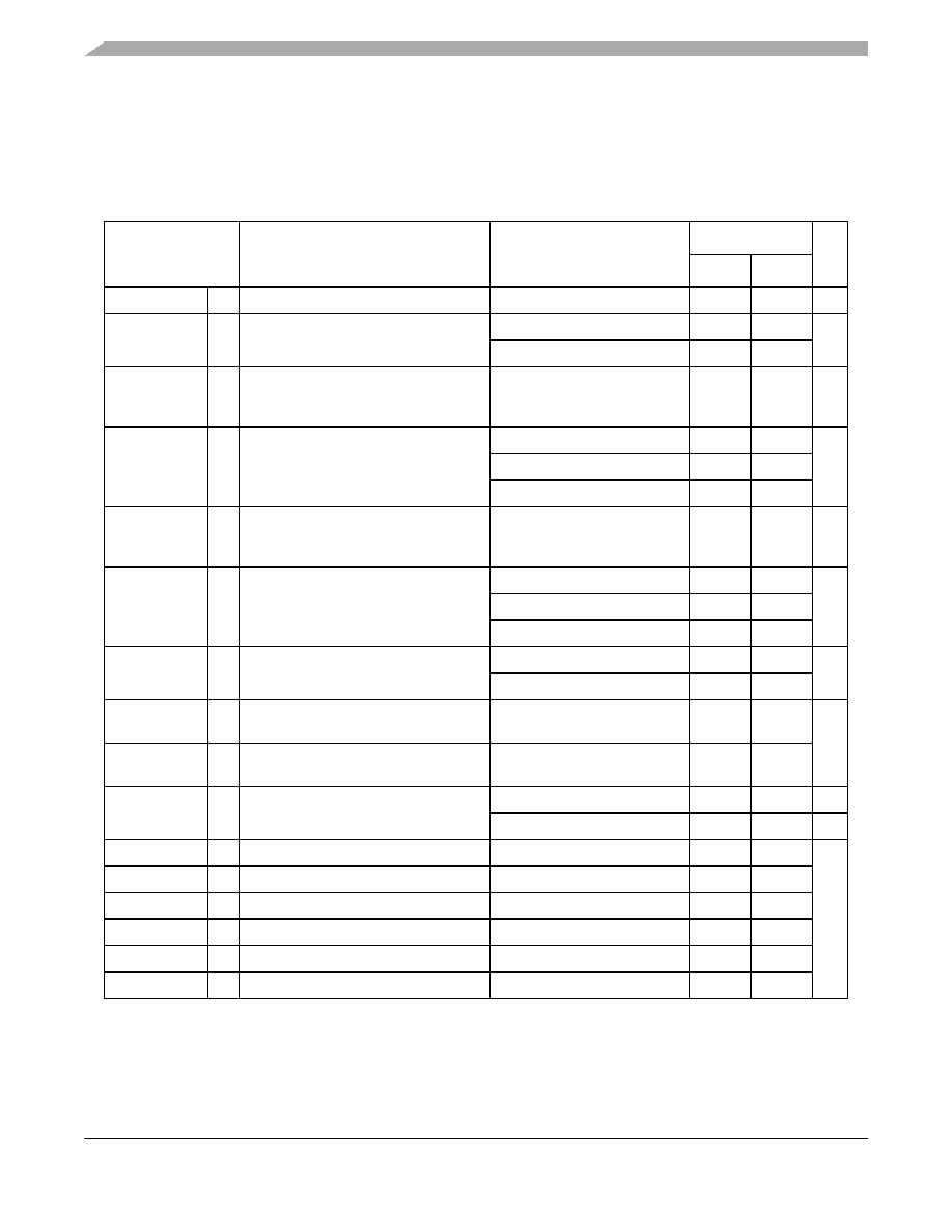
Table 8. Recommended operating conditions (5.0 V)
Symbol
Parameter
Conditions
Value
Unit
Min
Max
VSS
SR Digital ground on VSS_HV pins
—
0
V
VDD
1
SR Voltage on VDD_HV pins with respect to
ground (VSS)
—
4.5
5.5
V
Voltage drop2
3.0
5.5
VSS_LV
3
SR Voltage on VSS_LV (low voltage digital
supply) pins with respect to ground
(VSS)
—
VSS0.1 VSS+0.1
V
VDD_BV
4
SR Voltage on VDD_BV pin (regulator
supply) with respect to ground (VSS)
—
4.5
5.5
V
Voltage drop(2)
3.0
5.5
Relative to VDD
VDD0.1 VDD+0.1
VSS_ADC
SR Voltage on VSS_HV_ADC (ADC
reference) pin with respect to ground
(VSS
—
VSS0.1 VSS+0.1
V
VDD_ADC
5
SR Voltage on VDD_HV_ADC pin (ADC
reference) with respect to ground (VSS)
—
4.5
5.5
V
Voltage drop(2)
3.0
5.5
Relative to VDD
VDD0.1 VDD+0.1
VIN
SR Voltage on any GPIO pin with respect to
ground (VSS)
—
VSS0.1
—
V
Relative to VDD
—
VDD+0.1
IINJPAD
SR Injected input current on any pin during
overload condition
—
5
mA
IINJSUM
SR Absolute sum of all injected input
currents during overload condition
—
50
TVDD
SR VDD slope to ensure correct power up
6
—
0.25
V/s
—
3
—
V/s
TA C-Grade Part SR Ambient temperature under bias
fCPU < 64 MHz
40
85
°C
TJ C-Grade Part SR Junction temperature under bias
—
40
110
TA V-Grade Part
SR Ambient temperature under bias
fCPU < 64 MHz
40
105
TJ V-Grade Part
SR Junction temperature under bias
—
40
130
TA M-Grade Part SR Ambient temperature under bias
fCPU < 60 MHz
40
125
TJ M-Grade Part SR Junction temperature under bias
—
40
150
1 100 nF capacitance needs to be provided between each V
DD/VSS pair.
2 Full device operation is guaranteed by design when the voltage drops below 4.5V down to 3.6V. However, certain analog
electrical characteristics will not be guaranteed to stay within the stated limits.
3 330 nF capacitance needs to be provided between each V
DD_LV/VSS_LV supply pair.
Because
of
an
order
from
the
United
States
International
Trade
Commission,
BGA-packaged
product
lines
and
part
numbers
indicated
here
currently
are
not
available
from
Freescale
for
import
or
sale
in
the
United
States
prior
to
September
2010:
MPC5604BxMG
products
in
208
MAPBGA
packages
相關(guān)PDF資料 |
PDF描述 |
|---|---|
| MPC5602BEMLL | 32-BIT, FLASH, 60 MHz, MICROCONTROLLER, PQFP100 |
| MB89P475P-SH-201 | 8-BIT, OTPROM, 12.5 MHz, MICROCONTROLLER, PDIP48 |
| MCIMX31CVKN5D | 32-BIT, 532 MHz, MICROPROCESSOR, PBGA457 |
| MCIMX31LDVMN5D | 32-BIT, 532 MHz, MICROPROCESSOR, PBGA473 |
| MSP430F135IRTD | 16-BIT, FLASH, 8 MHz, RISC MICROCONTROLLER, PQCC64 |
相關(guān)代理商/技術(shù)參數(shù) |
參數(shù)描述 |
|---|---|
| MPC5602BEMLQ | 制造商:FREESCALE 制造商全稱:Freescale Semiconductor, Inc 功能描述:MPC5604B/C Microcontroller Data Sheet |
| MPC5602BEMLQR | 制造商:FREESCALE 制造商全稱:Freescale Semiconductor, Inc 功能描述:MPC5604B/C Microcontroller Data Sheet |
| MPC5602BEMLU | 制造商:FREESCALE 制造商全稱:Freescale Semiconductor, Inc 功能描述:Microcontroller |
| MPC5602BEMMG | 制造商:FREESCALE 制造商全稱:Freescale Semiconductor, Inc 功能描述:Microcontroller |
| MPC5602BEVLL | 制造商:FREESCALE 制造商全稱:Freescale Semiconductor, Inc 功能描述:MPC5604B/C Microcontroller Data Sheet |
發(fā)布緊急采購(gòu),3分鐘左右您將得到回復(fù)。