- 您現(xiàn)在的位置:買賣IC網(wǎng) > PDF目錄69036 > MPC5533MVZ40 (FREESCALE SEMICONDUCTOR INC) FLASH, 40 MHz, MICROCONTROLLER, PBGA324 PDF資料下載
參數(shù)資料
| 型號(hào): | MPC5533MVZ40 |
| 廠商: | FREESCALE SEMICONDUCTOR INC |
| 元件分類: | 微控制器/微處理器 |
| 英文描述: | FLASH, 40 MHz, MICROCONTROLLER, PBGA324 |
| 封裝: | 23 X 23 MM, 1 MM PITCH, LEAD FREE, MO-034AAJ-1, PLASTIC, TEPBGA-324 |
| 文件頁(yè)數(shù): | 31/50頁(yè) |
| 文件大小: | 1080K |
| 代理商: | MPC5533MVZ40 |
第1頁(yè)第2頁(yè)第3頁(yè)第4頁(yè)第5頁(yè)第6頁(yè)第7頁(yè)第8頁(yè)第9頁(yè)第10頁(yè)第11頁(yè)第12頁(yè)第13頁(yè)第14頁(yè)第15頁(yè)第16頁(yè)第17頁(yè)第18頁(yè)第19頁(yè)第20頁(yè)第21頁(yè)第22頁(yè)第23頁(yè)第24頁(yè)第25頁(yè)第26頁(yè)第27頁(yè)第28頁(yè)第29頁(yè)第30頁(yè)當(dāng)前第31頁(yè)第32頁(yè)第33頁(yè)第34頁(yè)第35頁(yè)第36頁(yè)第37頁(yè)第38頁(yè)第39頁(yè)第40頁(yè)第41頁(yè)第42頁(yè)第43頁(yè)第44頁(yè)第45頁(yè)第46頁(yè)第47頁(yè)第48頁(yè)第49頁(yè)第50頁(yè)
Electrical Characteristics
MPC5533 Microcontroller Data Sheet, Rev. 0.0
Freescale Semiconductor
37
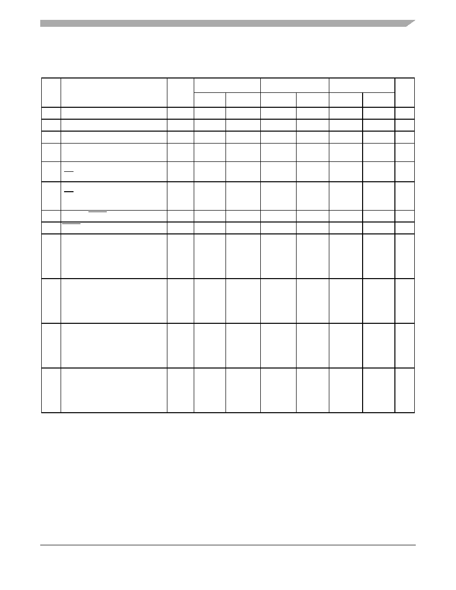
3.13.7
DSPI Timing
Table 25. DSPI Timing 1, 2
1 All DSPI timing specifications use the fastest slew rate (SRC = 0b11) on pad type M or MH. DSPI signals using pad types of
S or SH have an additional delay based on the slew rate. DSPI timing is specified at VDDEH = 3.0–5.25 V, TA = TL to TH, and
CL = 50 pF with SRC = 0b11.
2
Speed is the nominal maximum frequency. Max speed is the maximum speed allowed including frequency modulation (FM).
42 MHz parts allow for 40 MHz system clock + 2% FM; 68 MHz parts allow for a 66 MHz system clock + 2% FM, and
82 MHz parts allow for 80 MHz system clock + 2% FM.
Spec
Characteristic
Symbol
40 MHz
66 MHz
80 MHz
Unit
Min.
Max
Min.
Max
Min.
Max
1
SCK cycle time 3, 4
3 The minimum SCK cycle time restricts the baud rate selection for the given system clock rate.
These numbers are calculated based on two MPC55xx devices communicating over a DSPI link.
4 The actual minimum SCK cycle time is limited by pad performance.
tSCK
48.8 ns
5.8 ms
28.4 ns
3.5 ms
24.4 ns
2.9 ms
—
2
PCS to SCK delay5
5 The maximum value is programmable in DSPI_CTARx[PSSCK] and DSPI_CTARx[CSSCK].
tCSC
46
—26
—
22
—ns
3
After SCK delay6
6 The maximum value is programmable in DSPI_CTARx[PASC] and DSPI_CTARx[ASC].
tASC
45
—25
—
21
—ns
4
SCK duty cycle
tSDC
(tSCK ÷ 2)
– 2 ns
(tSCK ÷ 2)
+ 2 ns
(tSCK ÷ 2)
– 2 ns
(tSCK ÷ 2)
+ 2 ns
(tSCK ÷ 2)
– 2 ns
(tSCK ÷ 2)
+ 2 ns
ns
5
Slave access time
(SS active to SOUT driven)
tA
—
25
—
25
—
25
ns
6
Slave SOUT disable time
(SS inactive to SOUT Hi-Z, or
invalid)
tDIS
—
25
—
25
—
25
ns
7PCSx to PCSS time
tPCSC
4
—4
—
4
—ns
8PCSS to PCSx time
tPASC
5
—5
—
5
—ns
9
Data setup time for inputs
Master (MTFE = 0)
Slave
Master (MTFE = 1, CPHA = 0)7
Master (MTFE = 1, CPHA = 1)
7 This number is calculated using the SMPL_PT field in DSPI_MCR set to 0b10.
tSUI
20
2
–4
20
—
20
2
6
20
—
20
2
8
20
—
ns
10
Data hold time for inputs
Master (MTFE = 0)
Slave
Master (MTFE = 1, CPHA = 0)7
Master (MTFE = 1, CPHA = 1)
tHI
–4
7
45
–4
—
–4
7
25
–4
—
–4
7
21
–4
—
ns
11
Data valid (after SCK edge)
Master (MTFE = 0)
Slave
Master (MTFE = 1, CPHA = 0)
Master (MTFE = 1, CPHA = 1)
tSUO
—
5
25
45
5
—
5
25
5
—
5
25
21
5
ns
12
Data hold time for outputs
Master (MTFE = 0)
Slave
Master (MTFE = 1, CPHA = 0)
Master (MTFE = 1, CPHA = 1)
tHO
–5
5.5
8
–5
—
–5
5.5
4
–5
—
–5
5.5
3
–5
—
ns
相關(guān)PDF資料 |
PDF描述 |
|---|---|
| MPC5533MVF66 | FLASH, 66 MHz, MICROCONTROLLER, PBGA208 |
| MPC5565MZQ112 | 32-BIT, FLASH, 112 MHz, MICROCONTROLLER, PBGA324 |
| MPC5565MZQ132 | 32-BIT, FLASH, 132 MHz, MICROCONTROLLER, PBGA324 |
| MPC5565MVZ132 | 32-BIT, FLASH, 132 MHz, MICROCONTROLLER, PBGA324 |
| MPC5565MZQ80 | 32-BIT, FLASH, 80 MHz, MICROCONTROLLER, PBGA324 |
相關(guān)代理商/技術(shù)參數(shù) |
參數(shù)描述 |
|---|---|
| MPC5533MVZ66 | 制造商:FREESCALE 制造商全稱:Freescale Semiconductor, Inc 功能描述:Microcontroller Data Sheet |
| MPC5533MVZ80 | 制造商:FREESCALE 制造商全稱:Freescale Semiconductor, Inc 功能描述:Microcontroller Data Sheet |
| MPC5533MZQ40 | 制造商:FREESCALE 制造商全稱:Freescale Semiconductor, Inc 功能描述:Microcontroller Data Sheet |
| MPC5533MZQ66 | 制造商:FREESCALE 制造商全稱:Freescale Semiconductor, Inc 功能描述:Microcontroller Data Sheet |
| MPC5533MZQ80 | 制造商:FREESCALE 制造商全稱:Freescale Semiconductor, Inc 功能描述:Microcontroller Data Sheet |
發(fā)布緊急采購(gòu),3分鐘左右您將得到回復(fù)。