- 您現(xiàn)在的位置:買賣IC網(wǎng) > PDF目錄69035 > ML674001LA (OKI ELECTRIC INDUSTRY CO LTD) 32-BIT, MROM, 33.333 MHz, RISC MICROCONTROLLER, PBGA144 PDF資料下載
參數(shù)資料
| 型號: | ML674001LA |
| 廠商: | OKI ELECTRIC INDUSTRY CO LTD |
| 元件分類: | 微控制器/微處理器 |
| 英文描述: | 32-BIT, MROM, 33.333 MHz, RISC MICROCONTROLLER, PBGA144 |
| 封裝: | 11 X 11 MM, 0.80 MM PITCH, PLASTIC, LFBGA-144 |
| 文件頁數(shù): | 5/19頁 |
| 文件大?。?/td> | 645K |
| 代理商: | ML674001LA |
Oki Semiconductor 13
ML674001/ML67Q4002/ML67Q4003
April 2004, Rev 2.0
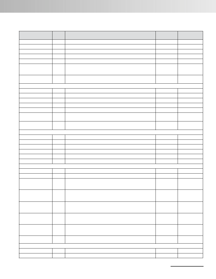
XOE_N
O
Output enable/ Read enable
–
Negative
XWE_N
O
Write enable
–
Negative
XBS_N[1:0]
O
Byte select: XBS_N[1] is for MSB, XBS_N[0] is for LSB
–
Negative
XBWE_N[0]
O
LSB Write enable
–
Negative
XBWE_N[1]
O
MSB Write enable
–
Negative
XWR
O
Data transfer direction for external bus, used when connecting to Motorola I/O devices.This
represent the secondary function of pin PIOC[7].
L = read, H = write. Available for I/O bank 0/1.
Secondary
–
XWAIT
I
External I/O bank 0/1, 2/3 WAIT signal.
This input permits access to devices slower than register settings.
Secondary
Positive
External bus control signals (EDO-DRAM/SDRAM)
XRAS_N
O
Row address strobe. Used for both EDO DRAM and SDRAM
Secondary
Negative
XCAS_N
O
Column address strobe signal (SDRAM)
Secondary
Negative
XSDCLK
O
SDRAM clock (same frequency as internal system clock)
Secondary
–
XSDCKE
O
Clock enable (SDRAM)
Secondary
–
XSDCS_N
O
Chip select (SDRAM)
Secondary
Negative
XDQM[1]/
XCAS_N[1]
O
Connected to SDRAM: DQM (MSB)
Connected to EDO-DRAM: column address strobe signal (MSB)
Secondary
Positive/
Negative
XDQM[0]/
XCAS_N[0]
O
Connected to SDRAM: DQM (LSB)
Connected to EDO-DRAM: column address strobe signal (LSB)
Secondary
Positive/
Negative
DMA control signals
DREQ[0]
I
Ch 0 DMA request signal, used when DMA controller congured for DREQ type
Secondary
Positive
DREQCLR[0]
O
Ch 0 DREQ signal clear request.The DMA device responds to this output by negating DREQ.
Secondary
Positive
TCOUT[0]
O
Indicates to Ch 0 DMA device that last transfer has started.
Secondary
Positive
DREQ[1]
I
Ch 1 DMA request signal, used when DMA controller congured for DREQ type.
Secondary
Positive
DREQCLR[1]
O
Ch 1 DREQ signal clear request.The DMA device responds to this output by negating DREQ.
Secondary
Positive
TCOUT[1]
O
Indicates to Ch 1 DMA device that last transfer has started.
Secondary
Positive
UART
SIN
I
UART receive signal.
Secondary
Positive
SOUT
O
UART transmit signal.
Secondary
Positive
CTS
I
Clear To Send.
Indicates that modem or data set is ready to transfer data. Bit 4 in the modem status reg-
ister reects this input.
Secondary
Negative
DSR
I
Data Set Ready.
Indicates that modem or data set is ready to establish a communications link with UART.
Bit 5 in the modem status register reects this input.
Secondary
Negative
DCD
I
Data Carrier Detect.
Indicates that modem or data set has detected data carrier signal. Bit 7 in the modem sta-
tus register reects this input.
Secondary
Negative
DTR
O
Data Terminal Ready.
Indicates that UART is ready to establish a communications link with the modem or data
set. Bit 0 in the modem control register controls this output.
Secondary
Negative
RTSO
Request To Send.
indicates that UART is ready to transfer data to modem or data set. Bit 1 in the modem
control register controls this output.
Secondary
Negative
RI
O
Ring Indicator. Indicates that the modem or data set has received a telephone ring indica-
tor. Bit 6 in the modem status register reects this input.
Secondary
Negative
SIO
STXD
O
SIO transmit signal
Secondary
Positive
SRXD
I
SIO receive signal
Secondary
Positive
Pin Descriptions (Continued)
Pin Name
I/O
Description
Primary/
Secondary
Logic
相關(guān)PDF資料 |
PDF描述 |
|---|---|
| ML67Q4051TC | RISC MICROCONTROLLER, PQFP144 |
| ML67Q4060TB | RISC MICROCONTROLLER, PQFP64 |
| ML67Q4050TC | RISC MICROCONTROLLER, PQFP144 |
| ML696201LA | 32-BIT, MROM, 120 MHz, RISC MICROCONTROLLER, PBGA272 |
| ML69Q6203LA | 32-BIT, FLASH, 120 MHz, RISC MICROCONTROLLER, PBGA272 |
相關(guān)代理商/技術(shù)參數(shù) |
參數(shù)描述 |
|---|---|
| ML674001TC | 制造商:ROHM Semiconductor 功能描述: |
| ML675001 | 制造商:OKI 制造商全稱:OKI electronic componets 功能描述:32-bit ARM-Based General-Purpose Microcontroller |
| ML675001ALAZ03A | 制造商:ROHM Semiconductor 功能描述:ARM7TDMI 32-BIT MCU 60 MHZ ROH |
| ML675001ATC | 制造商:ROHM Semiconductor 功能描述: |
| ML675001ATCZ03A | 制造商:ROHM Semiconductor 功能描述: |
發(fā)布緊急采購,3分鐘左右您將得到回復(fù)。