- 您現(xiàn)在的位置:買賣IC網(wǎng) > PDF目錄377971 > ML4875 (Fairchild Semiconductor Corporation) High Current Boost Regulator with Shutdown(帶關(guān)斷電路的大電流升壓穩(wěn)壓器) PDF資料下載
參數(shù)資料
| 型號(hào): | ML4875 |
| 廠商: | Fairchild Semiconductor Corporation |
| 英文描述: | High Current Boost Regulator with Shutdown(帶關(guān)斷電路的大電流升壓穩(wěn)壓器) |
| 中文描述: | 高電流升壓關(guān)斷穩(wěn)壓器(帶關(guān)斷電路的大電流升壓穩(wěn)壓器) |
| 文件頁(yè)數(shù): | 5/10頁(yè) |
| 文件大?。?/td> | 188K |
| 代理商: | ML4875 |
5
ML4875
FUNCTIONAL DESCRIPTION
The ML4875 combines Pulse Frequency Modulation
(PFM) and synchronous rectification to create a boost
converter that is both highly efficient and simple to use.
A PFM regulator charges a single inductor for a fixed
period of time and then completely discharges before
another cycle begins, simplifying the design by
eliminating the need for conventional current limiting
circuitry. Synchronous rectification is accomplished by
replacing an external Schottky diode with an on-chip
PMOS device, reducing switching losses and external
component count.
REGULATOR OPERATION
A block diagram of the boost converter is shown in Figure
2. The circuit remains idle when V
OUT
is at or above the
desired output voltage, drawing 50μA from V
IN
, and 8μA
from V
OUT
through the feedback resistors R1 and R2.
When V
OUT
drops below the desired output level, the
output of amplifier A1 goes high, signaling the regulator to
deliver charge to the output. Since the output of amplifier
A2 is normally high, the flip-flop captures the A1 set signal
and creates a pulse at the gate of the NMOS transistor Q1.
The NMOS transistor will charge the inductor L1 for 10μs,
resulting in a peak current given by:
I
T
V
L
s
L
V
L PEAK
(
ON
IN
IN
)
=
×
≈
×
1
1
10
μ
(1)
For reliable operation, L1 should be chosen so that I
L(PEAK)
does not exceed 1.5A.
When the one-shot times out, the NMOS transistor
releases the V
L
pin, allowing the inductor to fly-back and
momentarily charge the output through the body diode of
PMOS transistor Q2 in series with shutdown transistor Q3.
But, as the voltage across the PMOS transistor changes
polarity, its gate will be driven low by the current sense
amplifier A2, causing Q2 to short out its body diode. The
inductor then discharges into the load through Q2. The
output of A2 also serves to reset the flip-flop and one-shot
in preparation for the next charging cycle. A2 releases the
gate of Q2 when its current falls to zero. If V
OUT
is still
low, the flip-flop will immediately initiate another pulse.
The output capacitor (C1) filters the inductor current,
limiting output voltage ripple. Inductor current and one-
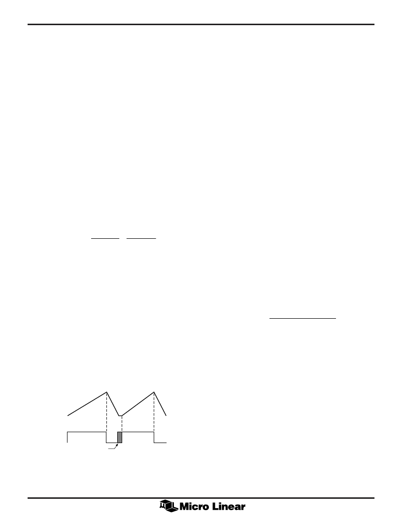
shot waveforms are shown in Figure 3.
Q(ONE SHOT)
Q1 ON
Q1 ON
Q2
ON
Q2
ON
INDUCTOR
CURRENT
Q1 & Q2 OFF
Figure 3. PFM Inductor Current Waveforms and Timing.
SHUTDOWN
The ML4875 output can be shut down by pulling the
SHDN pin high. When SHDN is high, the regulator stops
switching, the control circuitry is powered down, and the
body diode of the PMOS synchronous rectifier is
disconnected from the output, allowing the output voltage
to drop below the input voltage. This feature is unique to
the ML4875, as most boost regulators use external
Schottky diode rectifier which cannot be disconnected
during shutdown. Leaving the Schottky diode connected
causes excess power dissipation in the load during
shutdown because the Schottky conducts whenever the
output voltage drops 300mV below the input voltage.
RESET
COMPARATOR
An additional comparator is provided to detect low V
IN
,
or any other error condition that is important to the user.
The inverting input of the comparator is internally
connected to V
REF
, while the non-inverting input is
provided externally at the DETECT pin. The output of the
comparator is the
RESET
pin, which swings from V
OUT
to
GND when an error is detected.
DESIGN CONSIDERATIONS
INDUCTOR
Selecting the proper inductor for a specific application
usually involves a trade-off between efficiency and
maximum output current. Choosing too high a value will
keep the regulator from delivering the required output
current under worst case conditions. Choosing too low a
value causes efficiency to suffer. It is necessary to know
the maximum required output current and the input
voltage range to select the proper inductor value. The
maximum inductor value can be estimated using the
following formula:
L
V
T
×
V
I
MAX
I(
×
2
ON MIN
(
OUT
OUT MAX
(
=
×
×
)
)
)
2
η
(2)
where
h
is the efficiency, typically between 0.8 and 0.9.
Note that this is the value of inductance that just barely
delivers the required output current under worst case
conditions. A lower value may be required to cover
inductor tolerance, the effect of lower peak inductor
currents caused by resistive losses, and minimum dead
time between pulses.
Another method of determining the appropriate inductor
value is to make an estimate based on the typical
performance curves given in Figures 4 and 5. Figure 4
shows maximum output current as a function of input
voltage for several inductor values. These are typical
performance curves and leave no margin for inductance
and ON-time variations. To accommodate worst case
conditions, it is necessary to derate these curves by at
least 10% in addition to inductor tolerance.
For example, a two cell to 5V application requires 80mA
of output current while using an inductor with 15%
tolerance. The output current should be derated by 25%
to 100mA to cover the combined inductor and ON-time
相關(guān)PDF資料 |
PDF描述 |
|---|---|
| ML4876 | LCD Backlight Lamp Driver(LCD背光燈驅(qū)動(dòng)器) |
| ML4877 | LCD Desktop Backlight Lamp Driver(LCD桌面背光燈驅(qū)動(dòng)器) |
| ML4880 | Portable PC/PCMCIA Power Controller(便攜式PC/PCMCIA電源控制器) |
| ML4890 | High Efficiency, Low Ripple Boost Regulator(輸出可調(diào)、小波紋升壓穩(wěn)壓器) |
| ML4894 | Synchronous Buck Controller For DC/DC conversion(用于DC/DC變換的同步補(bǔ)償控制器(5.9V~15V到5V變換)) |
相關(guān)代理商/技術(shù)參數(shù) |
參數(shù)描述 |
|---|---|
| ML4875CS-3 | 制造商:Rochester Electronics LLC 功能描述: |
| ML4875CS-5 | 制造商:Rochester Electronics LLC 功能描述: |
| ML4875CS-T | 制造商:Rochester Electronics LLC 功能描述:- Tape and Reel |
| ML4875ES-3 | 制造商:MICRO-LINEAR 制造商全稱:MICRO-LINEAR 功能描述:Low Voltage Boost Regulator with Shutdown |
| ML4875ES-5 | 制造商:MICRO-LINEAR 制造商全稱:MICRO-LINEAR 功能描述:Low Voltage Boost Regulator with Shutdown |
發(fā)布緊急采購(gòu),3分鐘左右您將得到回復(fù)。