- 您現(xiàn)在的位置:買賣IC網(wǎng) > PDF目錄377971 > ML4841 (Fairchild Semiconductor Corporation) Variable Feedforward PFC/PWM Controller Combo(前饋可變PFC/PWM控制器組合芯片) PDF資料下載
參數(shù)資料
| 型號: | ML4841 |
| 廠商: | Fairchild Semiconductor Corporation |
| 英文描述: | Variable Feedforward PFC/PWM Controller Combo(前饋可變PFC/PWM控制器組合芯片) |
| 中文描述: | 可變前饋式PFC / PWM控制器組合(前饋可變式PFC /脈寬調(diào)制控制器組合芯片) |
| 文件頁數(shù): | 10/15頁 |
| 文件大?。?/td> | 149K |
| 代理商: | ML4841 |
ML4841
10
REV. 1.0 10/12/2000
FUNCTIONAL DESCRIPTION
(Continued)
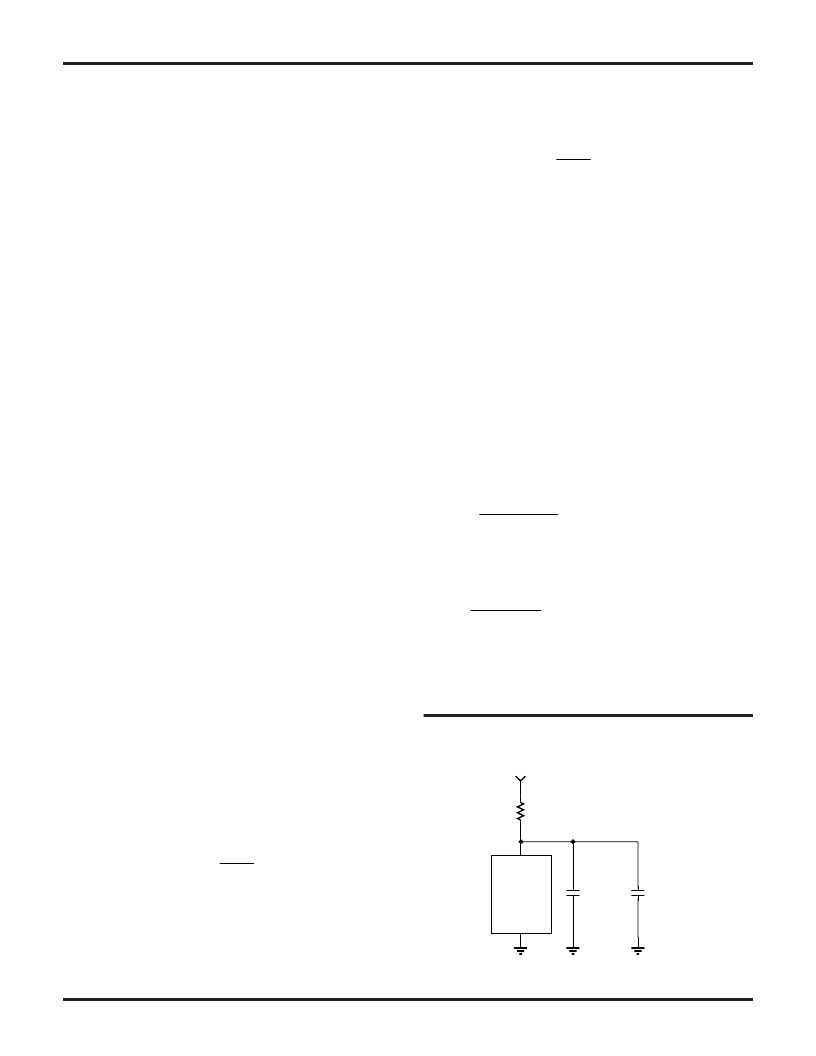
Figure 3. External Component Connections to V
CC
PFC buss can assist in line regulation accuracy and
response. As in current mode operation, the DC I
LIMIT
input would is used for output stage overcurrent
protection.
No voltage error amplifier is included in the PWM stage
of the ML4841, as this function is generally performed on
the output side of the PWM’s isolation boundary. To
facilitate the design of optocoupler feedback circuitry, an
offset has been built into the PWM’s RAMP 2 input which
allows V
DC
to command a zero percent duty cycle for
input voltages below 1.25V.
PWM Current Limit
The DC I
LIMIT
pin is a direct input to the cycle-by-cycle
current limiter for the PWM section. Should the input
voltage at this pin ever exceed 1V, the output of the PWM
will be disabled until the output flip-flop is reset by the
clock pulse at the start of the next PWM power cycle.
V
IN
OK Comparator
The V
IN
OK comparator monitors the DC output of the
PFC and inhibits the PWM if this voltage on V
FB
is less
than its nominal 2.5V. Once this voltage reaches 2.5V,
which corresponds to the PFC output capacitor being
charged to its rated boost voltage, the soft-start
commences.
PWM Control (RAMP 2)
When the PWM section is used in current mode, RAMP 2
is generally used as the sampling point for a voltage
representing the current in the primary of the PWM’s
output transformer, derived either by a current sensing
resistor or a current transformer. In voltage mode, it is the
input for a ramp voltage generated by a second set of
timing components (R
RAMP2
, C
RAMP2
), which will have a
minimum value of zero volts and should have a peak
value of approximately 5V. In voltage mode operation,
feedforward from the PFC output buss is an excellent way
to derive the timing ramp for the PWM stage.
Soft Start
Start-up of the PWM is controlled by the selection of the
external capacitor at SS. A current source of 50μA
supplies the charging current for the capacitor, and start-
up of the PWM begins at 1.25V. Start-up delay can be
programmed by the following equation:
(6)
where C
SS
is the required soft start capacitance, and
t
DELAY
is the desired start-up delay.
It is important that the time constant of the PWM soft-start
allow the PFC time to generate sufficient output power for
the PWM section. The PWM start-up delay should be at
least 5ms.
Solving for the minimum value of C
SS
:
Generating V
CC
The ML4841 is a current-fed part. It has an internal shunt
voltage regulator, which is designed to regulate the
voltage internal to the part at 13.5V. This allows a low
power dissipation while at the same time delivering 10V
of gate drive at the PWM OUT and PFC OUT outputs. It is
important to limit the current through the part to avoid
overheating or destroying it. This can be easily done with
a single resistor in series with the Vcc pin, returned to a
bias supply of typically 18V to 20V. The resistor’s value
must be chosen to meet the operating current requirement
of the ML4841 itself (19mA max) plus the current required
by the two gate driver outputs.
EXAMPLE:
With a V
BIAS
of 20V, a V
CC
limit of 14.6V (max) and
driving a total gate charge of 110nC at 100kHz (1 IRF840
MOSFET and 2 IRF830 MOSFETs), the gate driver current
required is:
I
kHz
nC
×
(
To check the maximum dissipation in the ML4841, check
the current at the minimum V
CC
(12.4V):
The maximum allowable I
CC
is 55mA, so this is an
acceptable design.
ML4841
VCC
GND
VBIAS
10nF
ceramic
1μF
ceramic
C
t
A
V
SS
DELAY
=
×
50
1 25
.
μ
C
ms
5
A
V
nF
SS
=
×
=
50
1 25
.
200
μ
kHz
nC
mA
GATEDRIVE
=
)
+
×
(
)
=
100
45
200
52
15
R
V
V
mA
mA
BIAS
=
+
=
20
19
14.
15
160
I
V
160
V
mA
CC
=
=
20
12.
47 5
.
相關(guān)PDF資料 |
PDF描述 |
|---|---|
| ML4851 | Low Current, Voltage Boost Regulator(小電流升壓穩(wěn)壓器) |
| ML4854IT | Adjustable, Low-Current, 2-Cell Boost Regulator with Shutdown and Low Battery Detect |
| ML4854 | Adjustable, Low-Current, 2-Cell Boost Regulator with Shutdown and Low Battery Detect |
| ML4861 | Low Voltage Drop Boost Regulator(低壓差升壓穩(wěn)壓器) |
| ML4863 | High Efficiency Flyback Controller(高效回轉(zhuǎn)電源控制器) |
相關(guān)代理商/技術(shù)參數(shù) |
參數(shù)描述 |
|---|---|
| ML4841CP | 功能描述:功率因數(shù)校正 IC PFC Controller PWM Combo RoHS:否 制造商:Fairchild Semiconductor 開關(guān)頻率:300 KHz 最大功率耗散: 最大工作溫度:+ 125 C 安裝風(fēng)格:SMD/SMT 封裝 / 箱體:SOIC-8 封裝:Reel |
| ML4841CP_Q | 功能描述:功率因數(shù)校正 IC PFC Controller PWM Combo RoHS:否 制造商:Fairchild Semiconductor 開關(guān)頻率:300 KHz 最大功率耗散: 最大工作溫度:+ 125 C 安裝風(fēng)格:SMD/SMT 封裝 / 箱體:SOIC-8 封裝:Reel |
| ML4841CS | 制造商:MICRO-LINEAR 制造商全稱:MICRO-LINEAR 功能描述:Variable Feedforward PFC/PWM Controller Combo |
| ML4841IP | 制造商:MICRO-LINEAR 制造商全稱:MICRO-LINEAR 功能描述:Variable Feedforward PFC/PWM Controller Combo |
| ML4841IS | 制造商:MICRO-LINEAR 制造商全稱:MICRO-LINEAR 功能描述:Variable Feedforward PFC/PWM Controller Combo |
發(fā)布緊急采購,3分鐘左右您將得到回復(fù)。