- 您現(xiàn)在的位置:買(mǎi)賣IC網(wǎng) > PDF目錄69033 > MK10N512VMB100R (FREESCALE SEMICONDUCTOR INC) FLASH, 100 MHz, RISC MICROCONTROLLER, PBGA81 PDF資料下載
參數(shù)資料
| 型號(hào): | MK10N512VMB100R |
| 廠商: | FREESCALE SEMICONDUCTOR INC |
| 元件分類: | 微控制器/微處理器 |
| 英文描述: | FLASH, 100 MHz, RISC MICROCONTROLLER, PBGA81 |
| 封裝: | 8 X 8 MM, MAPBGA-81 |
| 文件頁(yè)數(shù): | 28/64頁(yè) |
| 文件大?。?/td> | 1742K |
| 代理商: | MK10N512VMB100R |
第1頁(yè)第2頁(yè)第3頁(yè)第4頁(yè)第5頁(yè)第6頁(yè)第7頁(yè)第8頁(yè)第9頁(yè)第10頁(yè)第11頁(yè)第12頁(yè)第13頁(yè)第14頁(yè)第15頁(yè)第16頁(yè)第17頁(yè)第18頁(yè)第19頁(yè)第20頁(yè)第21頁(yè)第22頁(yè)第23頁(yè)第24頁(yè)第25頁(yè)第26頁(yè)第27頁(yè)當(dāng)前第28頁(yè)第29頁(yè)第30頁(yè)第31頁(yè)第32頁(yè)第33頁(yè)第34頁(yè)第35頁(yè)第36頁(yè)第37頁(yè)第38頁(yè)第39頁(yè)第40頁(yè)第41頁(yè)第42頁(yè)第43頁(yè)第44頁(yè)第45頁(yè)第46頁(yè)第47頁(yè)第48頁(yè)第49頁(yè)第50頁(yè)第51頁(yè)第52頁(yè)第53頁(yè)第54頁(yè)第55頁(yè)第56頁(yè)第57頁(yè)第58頁(yè)第59頁(yè)第60頁(yè)第61頁(yè)第62頁(yè)第63頁(yè)第64頁(yè)
6.6.1 ADC electrical specifications
differential pins ADCx_DP0, ADCx_DM0, ADCx_DP1, ADCx_DM1, ADCx_DP3, and
ADCx_DP3.
The ADCx_DP2 and ADCx_DM2 ADC inputs are used as the PGA inputs and are not
direct device pins. Accuracy specifications for these pins are defined in Table 26 and
All other ADC channels meet the 13-bit differential/12-bit single-ended accuracy
specifications.
6.6.1.1 16-bit ADC operating conditions
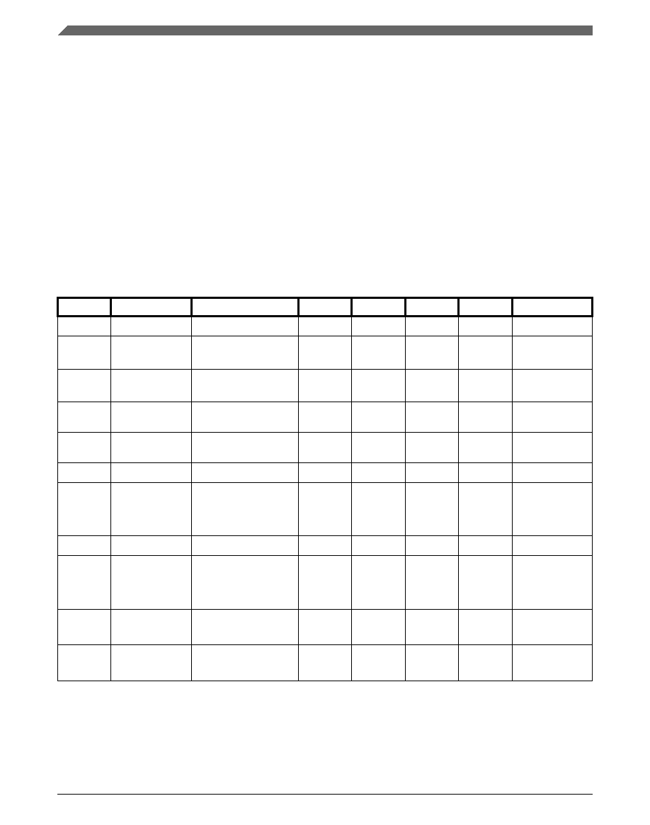
Table 24. 16-bit ADC operating conditions
Symbol
Description
Conditions
Min.
Max.
Unit
Notes
VDDA
Supply voltage
Absolute
1.71
—
3.6
V
ΔVDDA
Supply voltage
Delta to VDD (VDD-
VDDA)
-100
0
+100
mV
ΔVSSA
Ground voltage
Delta to VSS (VSS-
VSSA)
-100
0
+100
mV
VREFH
ADC reference
voltage high
1.13
VDDA
V
VREFL
Reference
voltage low
VSSA
V
VADIN
Input voltage
VREFL
—
VREFH
V
CADIN
Input
capacitance
16 bit modes
8/10/12 bit
modes
—
8
4
10
5
pF
RADIN
Input resistance
—
2
5
kΩ
RAS
Analog source
resistance
13/12 bit modes
fADCK < 4MHz
—
5
kΩ
fADCK
ADC conversion
clock frequency
≤13 bit modes
1.0
—
18.0
MHz
fADCK
ADC conversion
clock frequency
16 bit modes
2.0
—
12.0
MHz
Table continues on the next page...
Peripheral operating requirements and behaviors
K10 Sub-Family Data Sheet Data Sheet, Rev. 4, 3/2011.
34
Preliminary
Freescale Semiconductor, Inc.
相關(guān)PDF資料 |
PDF描述 |
|---|---|
| MK10N512VLK100 | FLASH, 100 MHz, RISC MICROCONTROLLER, PQFP80 |
| MK10N512VML100 | RISC MICROCONTROLLER, PBGA104 |
| MK10X512VLQ100 | RISC MICROCONTROLLER, PQFP144 |
| MK10X512VMD100 | RISC MICROCONTROLLER, PBGA144 |
| MK1493-02AGTR | 200 MHz, PROC SPECIFIC CLOCK GENERATOR, PDSO56 |
相關(guān)代理商/技術(shù)參數(shù) |
參數(shù)描述 |
|---|---|
| MK10N512VMB120 | 制造商:FREESCALE 制造商全稱:Freescale Semiconductor, Inc 功能描述:K10 Sub-Family Data Sheet |
| MK10N512VMB120R | 制造商:FREESCALE 制造商全稱:Freescale Semiconductor, Inc 功能描述:K10 Sub-Family Data Sheet |
| MK10N512VMB150 | 制造商:FREESCALE 制造商全稱:Freescale Semiconductor, Inc 功能描述:K10 Sub-Family Data Sheet |
| MK10N512VMB150R | 制造商:FREESCALE 制造商全稱:Freescale Semiconductor, Inc 功能描述:K10 Sub-Family Data Sheet |
| MK10N512VMB50 | 制造商:FREESCALE 制造商全稱:Freescale Semiconductor, Inc 功能描述:K10 Sub-Family Data Sheet |
發(fā)布緊急采購(gòu),3分鐘左右您將得到回復(fù)。