- 您現(xiàn)在的位置:買賣IC網(wǎng) > PDF目錄182421 > MJB5742T4G (ON SEMICONDUCTOR) 8 A, 400 V, NPN, Si, POWER TRANSISTOR PDF資料下載
參數(shù)資料
| 型號(hào): | MJB5742T4G |
| 廠商: | ON SEMICONDUCTOR |
| 元件分類: | 功率晶體管 |
| 英文描述: | 8 A, 400 V, NPN, Si, POWER TRANSISTOR |
| 封裝: | ROHS COMPLIANT, CASE 418B-04, D2PAK-3 |
| 文件頁(yè)數(shù): | 5/7頁(yè) |
| 文件大小: | 126K |
| 代理商: | MJB5742T4G |
MJB5742T4G
http://onsemi.com
5
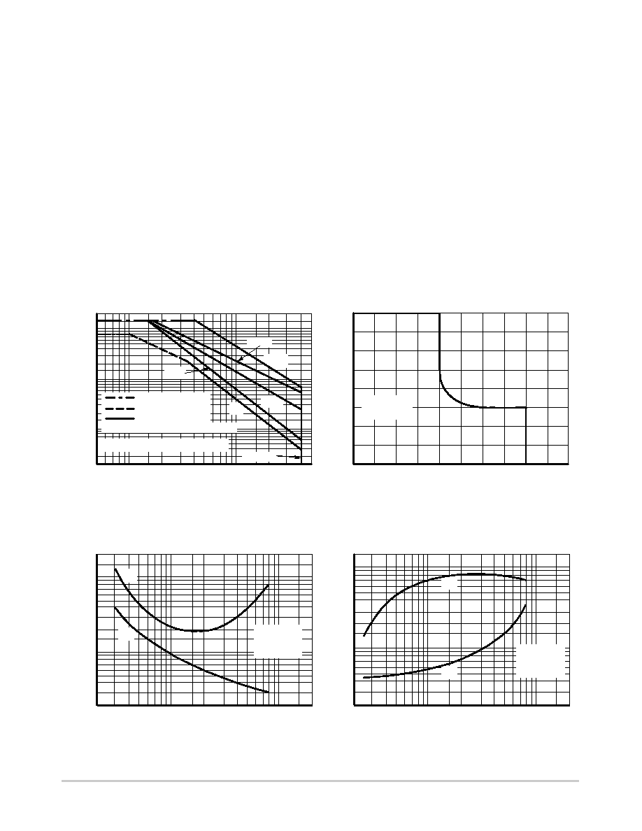
SAFE OPERATING AREA INFORMATION
FORWARD BIAS
There are two limitations on the power handling ability of
a transistor: average junction temperature and second
breakdown. Safe operating area curves indicate IC VCE
limits of the transistor that must be observed for reliable
operation; i.e., the transistor must not be subjected to greater
dissipation than the curves indicate.
variable depending on power level. Second breakdown
pulse limits are valid for duty cycles to 10% but must be
derated when TC ≥ 25_C. Second breakdown limitations do
not derate the same as thermal limitations. Allowable
current at the voltages shown on Figure 6 may be found at
any case temperature by using the appropriate curve on
Figure 1.
REVERSE BIAS
For inductive loads, high voltage and high current must be
sustained simultaneously during turnoff, in most cases,
with the base to emitter junction reverse biased. Under these
conditions the collector voltage must be held to a safe level
at or below a specific value of collector current. This can be
accomplished by several means such as active clamping, RC
snubbing, load line shaping, etc. The safe level for these
devices is specified as Reverse Bias Safe Operating Area
and represents the voltagecurrent condition allowable
during reverse biased turnoff. This rating is verified under
clamped conditions so that the device is never subjected to
an avalanche mode. Figure 7 gives the complete RBSOA
characteristics.
The Safe Operating Area figures shown in Figures 6 and 7 are specified ratings for these devices under the test conditions shown.
I C
,COLLECT
OR
CURRENT
(AMPS)
VCE, COLLECTOR-EMITTER VOLTAGE (VOLTS)
Figure 6. Forward Bias Safe Operating Area
Figure 7. Reverse Bias Safe Operating Area
16
14
12
8
0
2
4
10
100
200
300
500
0
400
16
5
10
8
1
0.02
100
I C
,COLLECT
OR
CURRENT
(AMPS)
0.1
10
20
200
400
3
0.5
50
0.3
0.05
dc
1ms
100
ms
MJB5742
VBE(off) ≤ 5 V
TJ = 100°C
6
CURVES APPLY BELOW RATED VCEO
10
ms
5ms
BONDING WIRE LIMIT
THERMAL LIMIT
(SINGLE PULSE)
SECOND BREAKDOWN LIMIT
t,TIME
(s)μ
t,TIME
(s)μ
IC, COLLECTOR CURRENT (AMPS)
0.5 0.7
1
2
10
7
5
2
1
0.7
0.2
0.3
5
0.5
10
3
0.3
0.2
7
IC, COLLECTOR CURRENT (AMPS)
0.5 0.7
1
2
10
0.7
0.5
0.2
0.1
0.07
0.02
0.3
Figure 8. TurnOn Time
5
0.05
1
Figure 9. TurnOff Time
3
VCC = 250 V
IB1 = IB2
IC/IB = 20
ts
tr
tf
td
VCC = 250 V
IB1 = IB2
IC/IB = 20
0.3
0.03
0.2
7
RESISTIVE SWITCHING PERFORMANCE
相關(guān)PDF資料 |
PDF描述 |
|---|---|
| MJD112I | 2 A, 100 V, NPN, Si, POWER TRANSISTOR |
| MJD117-1 | 2 A, 100 V, PNP, Si, POWER TRANSISTOR |
| MJD117T4 | 2 A, 100 V, PNP, Si, POWER TRANSISTOR |
| MJD112-1 | 2 A, 100 V, NPN, Si, POWER TRANSISTOR |
| MJD117 | 2 A, 100 V, PNP, Si, POWER TRANSISTOR |
相關(guān)代理商/技術(shù)參數(shù) |
參數(shù)描述 |
|---|---|
| MJB61861801 | 制造商:LG Corporation 功能描述:Stopper,Compressor |
| MJB61872001 | 制造商:LG Corporation 功能描述:Stopper,Slide |
| MJB61872101 | 制造商:LG Corporation 功能描述:Stopper,Slide |
| MJB61872201 | 制造商:LG Corporation 功能描述:Stopper,Slide |
| MJB61877901 | 制造商:LG Corporation 功能描述:Stopper,Compressor |
發(fā)布緊急采購(gòu),3分鐘左右您將得到回復(fù)。