- 您現(xiàn)在的位置:買賣IC網 > PDF目錄1953 > MCW1001AT-I/SS (Microchip Technology)IC INTERFACE SOCKET XLP 28-SSOP PDF資料下載
參數(shù)資料
| 型號: | MCW1001AT-I/SS |
| 廠商: | Microchip Technology |
| 文件頁數(shù): | 9/66頁 |
| 文件大?。?/td> | 0K |
| 描述: | IC INTERFACE SOCKET XLP 28-SSOP |
| 標準包裝: | 2,100 |
| 系列: | * |
第1頁第2頁第3頁第4頁第5頁第6頁第7頁第8頁當前第9頁第10頁第11頁第12頁第13頁第14頁第15頁第16頁第17頁第18頁第19頁第20頁第21頁第22頁第23頁第24頁第25頁第26頁第27頁第28頁第29頁第30頁第31頁第32頁第33頁第34頁第35頁第36頁第37頁第38頁第39頁第40頁第41頁第42頁第43頁第44頁第45頁第46頁第47頁第48頁第49頁第50頁第51頁第52頁第53頁第54頁第55頁第56頁第57頁第58頁第59頁第60頁第61頁第62頁第63頁第64頁第65頁第66頁
2011 Microchip Technology Inc.
Preliminary
DS70671A-page 17
MCW1001A
2.5
GPIO PINS
When developing an application, the capabilities of the
port pins must be considered. Outputs on some pins
have higher output drive strength than others. Similarly,
some pins can tolerate higher than VDD input levels.
2.5.1
INPUT PINS AND VOLTAGE
CONSIDERATIONS
The voltage tolerance of the GPIO pins varies across
the bank of pins. Some of the pins when used as digital
only inputs can handle DC voltages up to 5.5V, a level
typical for digital logic circuits. Table summarizes the
input voltage capabilities of the I/O pins. For more infor-
mation on electrical characteristic, refer to Section 7.0,
Electrical Characteristics. Voltage excursions beyond
VDD on these pins should be avoided.
TABLE 2-1:
INPUT VOLTAGE LEVELS
2.5.2
PIN OUTPUT DRIVE
The GPIO output pin drive strength varies across the
GPIO bank of pins to meet the needs of a variety of
applications. There are two classes of output pins in
terms of drive capability.
GPIO<5:7> – Designed to drive higher current
loads, such as LED's.
GPIO<0:4> – Designed for small loads, typically
indication only. Table 2-2 summarizes the output
capabilities. For more information, refer to the
TABLE 2-2:
OUTPUT DRIVE LEVELS
:
2.5.3
INTERFACING TO A +5V SYSTEM
Though the VDDMAX of the MCW1001A is 3.6V, this
device is still capable of interfacing with 5V systems,
even if the VIH of the target system is above 3.6V. This
is accomplished by adding a pull-up resistor to the
GPIO pin, see Figure 2-2. To produce a high output, the
GPIO pin must be configured as an input, and to
produce a low output, the GPIO pin must be configured
as an output and set low. Only GPIO pins that are
tolerant of voltages up to 5.5V can be used for this type
of interface.
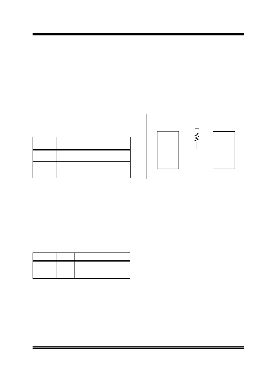
FIGURE 2-2:
+5V SYSTEM HARDWARE
INTERFACE
Pin
Tolerated
Input
Description
GPIO<0:4>
VDD
Only VDD input levels are
tolerated.
GPIO<5:7>
5.5V
Tolerates input levels above
VDD and useful for most
standard logic.
Pin
Drive
Description
GPIO<0:4> Medium Intended for indication.
GPIO<5:7>
High
Suitable for direct LED drive
levels.
GPIO1
+5V Device
+5V
MCW1001A
相關PDF資料 |
PDF描述 |
|---|---|
| MCZ145010EG | IC SMOKE DETECT PHOTOELEC 16SOIC |
| MCZ145012EG | IC SMOKE DETECT PHOTOELEC 16SOIC |
| MCZ33094EG | IC IGNITION CONTROL 12V 16-SOIC |
| MCZ33287EG | IC DRIVER DUAL LOSIDE MON 20SOIC |
| MCZ33290EF | IC SER LNK INTER ISO KLINE 8SOIC |
相關代理商/技術參數(shù) |
參數(shù)描述 |
|---|---|
| MCW1011 | 制造商:MINMAX 制造商全稱:Minmax Technology Co., Ltd. 功能描述:2W, Wide Input Range SIP, Single Output DC/DC Converters |
| MCW1012 | 制造商:MINMAX 制造商全稱:Minmax Technology Co., Ltd. 功能描述:2W, Wide Input Range SIP, Single Output DC/DC Converters |
| MCW1013 | 制造商:MINMAX 制造商全稱:Minmax Technology Co., Ltd. 功能描述:2W, Wide Input Range SIP, Single Output DC/DC Converters |
| MCW1021 | 制造商:MINMAX 制造商全稱:Minmax Technology Co., Ltd. 功能描述:2W, Wide Input Range SIP, Single Output DC/DC Converters |
| MCW1022 | 制造商:MINMAX 制造商全稱:Minmax Technology Co., Ltd. 功能描述:2W, Wide Input Range SIP, Single Output DC/DC Converters |
發(fā)布緊急采購,3分鐘左右您將得到回復。