- 您現(xiàn)在的位置:買賣IC網(wǎng) > PDF目錄296503 > MCP607-I/SNG DUAL OP-AMP, 250 uV OFFSET-MAX, 0.155 MHz BAND WIDTH, PDSO8 PDF資料下載
參數(shù)資料
| 型號: | MCP607-I/SNG |
| 元件分類: | 運(yùn)算放大器 |
| 英文描述: | DUAL OP-AMP, 250 uV OFFSET-MAX, 0.155 MHz BAND WIDTH, PDSO8 |
| 封裝: | 3.90 MM, PLASTIC, SOIC-8 |
| 文件頁數(shù): | 8/42頁 |
| 文件大小: | 690K |
| 代理商: | MCP607-I/SNG |
第1頁第2頁第3頁第4頁第5頁第6頁第7頁當(dāng)前第8頁第9頁第10頁第11頁第12頁第13頁第14頁第15頁第16頁第17頁第18頁第19頁第20頁第21頁第22頁第23頁第24頁第25頁第26頁第27頁第28頁第29頁第30頁第31頁第32頁第33頁第34頁第35頁第36頁第37頁第38頁第39頁第40頁第41頁第42頁
MCP606/7/8/9
DS11177F-page 16
2009 Microchip Technology Inc.
4.2
Rail-to-Rail Output
There are two
specifications
that
describe
the
output-swing capability of the MCP606/7/8/9 family of
op amps. The first specification (Maximum Output
Voltage Swing) defines the absolute maximum swing
that can be achieved under the specified load
conditions. For instance, the output voltage swings to
within 15 mV of the negative rail with a 25 k
Ω load to
limited when the input goes beyond the linear region of
operation.
The second specification that describes the output-
swing capability of these amplifiers (Linear Output
Voltage Range) defines the maximum output swing that
can be achieved while the amplifier still operates in its
linear region. To verify linear operation in this range, the
large-signal DC Open-Loop Gain (AOL) is measured at
points inside the supply rails. The measurement must
meet the specified AOL conditions in the specification
table.
4.3
Capacitive Loads
Driving large capacitive loads can cause stability
problems for voltage-feedback op amps. As the load
capacitance increases, the feedback loop’s phase
margin decreases and the closed-loop bandwidth is
reduced. This produces gain-peaking in the frequency
response, with overshoot and ringing in the step
response. A unity-gain buffer (G = +1) is the most
sensitive to capacitive loads, though all gains show the
same general behavior.
When driving large capacitive loads with these op
amps (e.g., > 60 pF when G = +1), a small series
feedback loop’s phase margin (stability) by making the
output load resistive at higher frequencies. The
bandwidth will be generally lower than the bandwidth
with no capacitive load.
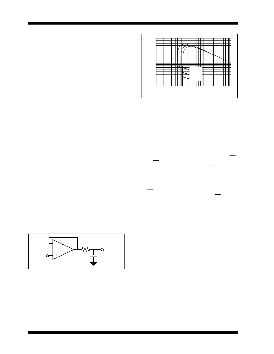
FIGURE 4-4:
Output Resistor, RISO
stabilizes large capacitive loads.
different capacitive loads and gains. The x-axis is the
normalized load capacitance (CL/GN), where GN is the
circuit’s noise gain. For non-inverting gains, GN and the
Signal Gain are equal. For inverting gains, GN is
1+|Signal Gain| (e.g., -1 V/V gives GN =+2V/V).
FIGURE 4-5:
Recommended RISO Values
for Capacitive Loads.
After selecting RISO for your circuit, double-check the
resulting
frequency
response
peaking
and
step
response overshoot. Modify RISO’s value until the
response is reasonable. Bench evaluation and simula-
tions with the MCP606/7/8/9 SPICE macro model are
helpful.
4.4
MCP608 Chip Select
The MCP608 is a single op amp with Chip Select (CS).
When CS is pulled high, the supply current drops to
50 nA (typical) and flows through the CS pin to VSS.
When this happens, the amplifier output is put into a
high-impedance state. By pulling CS low, the amplifier
is enabled. The CS pin has an internal 5 M
Ω (typical)
pull-down resistor connected to VSS, so it will go low if
the CS pins is left floating. Figure 1-1 shows the output
voltage and supply current response to a CS pulse.
4.5
Supply Bypass
With this family of operational amplifiers, the power
supply pin (VDD for single-supply) should have a local
bypass capacitor (i.e., 0.01 F to 0.1 F) within 2 mm
for good high-frequency performance. It also needs a
bulk capacitor (i.e., 1 F or larger) within 100 mm to
provide large, slow currents. This bulk capacitor can be
shared with other nearby analog parts.
VIN
RISO
VOUT
CL
MCP60X
100
1000
10000
10
100
1000
10000
Normalized Load Capacitance; CL/GN (F)
Recommended
R
ISO
(
)
10p
10n
1n
100p
100
10k
1k
GN = +1
GN = +2
GN ≥ +4
相關(guān)PDF資料 |
PDF描述 |
|---|---|
| MCP6142-E/MS | DUAL OP-AMP, 3000 uV OFFSET-MAX, 0.1 MHz BAND WIDTH, PDSO8 |
| MCP631-E/SN | OP-AMP, 8000 uV OFFSET-MAX, 24 MHz BAND WIDTH, PDSO8 |
| MCP631T-E/SN | OP-AMP, 8000 uV OFFSET-MAX, 24 MHz BAND WIDTH, PDSO8 |
| MCP73832-4ADI/OT | 1-CHANNEL POWER SUPPLY SUPPORT CKT, PDSO5 |
| MCP73832-5DCI/MC | 1-CHANNEL POWER SUPPLY SUPPORT CKT, PDSO8 |
相關(guān)代理商/技術(shù)參數(shù) |
參數(shù)描述 |
|---|---|
| MCP607T | 制造商:MICROCHIP 制造商全稱:Microchip Technology 功能描述:2.5V to 6.0V Micropower CMOS Op Amp |
| MCP607TI/OT | 制造商:MICROCHIP 制造商全稱:Microchip Technology 功能描述:2.5V TO 5.5V MICROPOWER CMOS OP AMPS |
| MCP607TI/P | 制造商:MICROCHIP 制造商全稱:Microchip Technology 功能描述:2.5V TO 5.5V MICROPOWER CMOS OP AMPS |
| MCP607TI/SL | 制造商:MICROCHIP 制造商全稱:Microchip Technology 功能描述:2.5V TO 5.5V MICROPOWER CMOS OP AMPS |
| MCP607TI/SN | 制造商:MICROCHIP 制造商全稱:Microchip Technology 功能描述:2.5V TO 5.5V MICROPOWER CMOS OP AMPS |
發(fā)布緊急采購,3分鐘左右您將得到回復(fù)。