- 您現(xiàn)在的位置:買賣IC網(wǎng) > PDF目錄9335 > MCP4162T-104E/MS (Microchip Technology)IC POT DGTL SNGL 100K RHEO 8MSOP PDF資料下載
第1頁第2頁第3頁第4頁第5頁第6頁第7頁第8頁第9頁第10頁第11頁第12頁第13頁第14頁第15頁第16頁第17頁第18頁第19頁第20頁第21頁第22頁第23頁第24頁第25頁第26頁第27頁第28頁第29頁第30頁第31頁第32頁第33頁第34頁第35頁當前第36頁第37頁第38頁第39頁第40頁第41頁第42頁第43頁第44頁第45頁第46頁第47頁第48頁第49頁第50頁第51頁第52頁第53頁第54頁第55頁第56頁第57頁第58頁第59頁第60頁第61頁第62頁第63頁第64頁第65頁第66頁第67頁第68頁第69頁第70頁第71頁第72頁第73頁第74頁第75頁第76頁第77頁第78頁第79頁第80頁第81頁第82頁第83頁第84頁第85頁第86頁第87頁第88頁

2008 Microchip Technology Inc.
DS22059B-page 41
MCP414X/416X/424X/426X
6.1.4
SERIAL CLOCK (SCK)
(SPI FREQUENCY OF OPERATION)
The SPI interface is specified to operate up to 10 MHz.
The actual clock rate depends on the configuration of
the system and the serial command used. Table 6-1
shows the SCK frequency for different configurations.
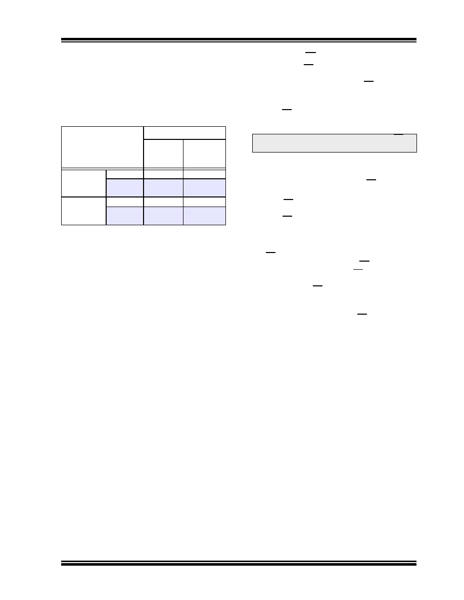
TABLE 6-1:
SCK FREQUENCY
6.1.5
THE CS SIGNAL
The Chip Select (CS) signal is used to select the device
and frame a command sequence. To start a command,
or sequence of commands, the CS signal must
transition from the inactive state (VIH) to an active state
(VIL or VIHH).
After the CS signal has gone active, the SDO pin is
driven and the clock bit counter is reset.
If an error condition occurs for an SPI command, then
the Command byte’s Command Error (CMDERR) bit
(on the SDO pin) will be driven low (VIL). To exit the
error condition, the user must take the CS pin to the VIH
level.
When the CS pin returns to the inactive state (VIH) the
SPI module resets (including the address pointer).
While the CS pin is in the inactive state (VIH), the serial
interface is ignored. This allows the Host Controller to
interface to other SPI devices using the same SDI,
SDO, and SCK signals.
The CS pin has an internal pull-up resistor. The resistor
is disabled when the voltage on the CS pin is at the VIL
level. This means that when the CS pin is not driven,
the internal pull-up resistor will pull this signal to the VIH
level.
When the CS pin is driven low (VIL), the
resistance becomes very large to reduce the device
current consumption.
The high voltage capability of the CS pin allows High
Voltage commands. High Voltage commands allow the
device’s WiperLock Technology and write protect
features to be enabled and disabled.
Memory Type Access
Command
Read
Write,
Increment,
Decrement
Non-Volatile
Memory
SDI, SDO
10 MHz
10 MHz (2, 3)
SDI/SDO
(1)
250 kHz (4) 10 MHz (2, 3)
Volatile
Memory
SDI, SDO
10 MHz
SDI/SDO
(1)
250 kHz (4)
10 MHz
Note 1:
MCP41X1 devices only
2:
Non-Volatile memory does not support
the Increment or Decrement command.
3:
After a Write command, the internal write
cycle must complete before the next SPI
command is received.
4:
This is the maximum clock frequency
without an external pull-up resistor.
Note:
There is a required delay after the CS pin
goes active to the 1st edge of the SCK pin.
相關PDF資料 |
PDF描述 |
|---|---|
| VI-21T-MX-B1 | CONVERTER MOD DC/DC 6.5V 75W |
| X1288S16I-4.5AT1 | IC RTC/CAL/CPU SUP EE 16-SOIC |
| MCP4161T-103E/MS | IC POT DGTL SNGL 10K SPI 8MSOP |
| VE-B1W-MV | CONVERTER MOD DC/DC 5.8V 150W |
| X1288S16I-4.5A | IC RTC/CAL/CPU SUP EE 16-SOIC |
相關代理商/技術參數(shù) |
參數(shù)描述 |
|---|---|
| MCP4162T-104I/MF | 制造商:MICROCHIP 制造商全稱:Microchip Technology 功能描述:7/8-Bit Single/Dual SPI Digital POT with Non-Volatile Memory |
| MCP4162T-104I/ML | 制造商:MICROCHIP 制造商全稱:Microchip Technology 功能描述:7/8-Bit Single/Dual SPI Digital POT with Non-Volatile Memory |
| MCP4162T-104I/MS | 制造商:MICROCHIP 制造商全稱:Microchip Technology 功能描述:7/8-Bit Single/Dual SPI Digital POT with Non-Volatile Memory |
| MCP4162T-104I/P | 制造商:MICROCHIP 制造商全稱:Microchip Technology 功能描述:7/8-Bit Single/Dual SPI Digital POT with Non-Volatile Memory |
| MCP4162T-104I/SL | 制造商:MICROCHIP 制造商全稱:Microchip Technology 功能描述:7/8-Bit Single/Dual SPI Digital POT with Non-Volatile Memory |
發(fā)布緊急采購,3分鐘左右您將得到回復。