- 您現(xiàn)在的位置:買賣IC網(wǎng) > PDF目錄296503 > MCP1700T-3302ETO (Microchip Technology Inc.) Low Quiescent Current LDO PDF資料下載
參數(shù)資料
| 型號: | MCP1700T-3302ETO |
| 廠商: | Microchip Technology Inc. |
| 元件分類: | 線性穩(wěn)壓 |
| 英文描述: | Low Quiescent Current LDO |
| 中文描述: | 低靜態(tài)電流低壓降穩(wěn)壓器 |
| 文件頁數(shù): | 18/24頁 |
| 文件大小: | 638K |
| 代理商: | MCP1700T-3302ETO |
2007 Microchip Technology Inc.
DS21826B-page 3
MCP1700
1.0
ELECTRICAL
CHARACTERISTICS
Absolute Maximum Ratings
VDD............................................................................................+6.5V
All inputs and outputs w.r.t. .............(VSS-0.3V) to (VIN+0.3V)
Peak Output Current .................................... Internally Limited
Storage temperature .....................................-65°C to +150°C
Maximum Junction Temperature................................... 150°C
Operating Junction Temperature...................-40°C to +125°C
ESD protection on all pins (HBM;MM)
............... ≥ 4kV; ≥ 400V
Notice: Stresses above those listed under “Maximum
Ratings” may cause permanent damage to the device. This is
a stress rating only and functional operation of the device at
those or any other conditions above those indicated in the
operational listings of this specification is not implied.
Exposure to maximum rating conditions for extended periods
may affect device reliability.
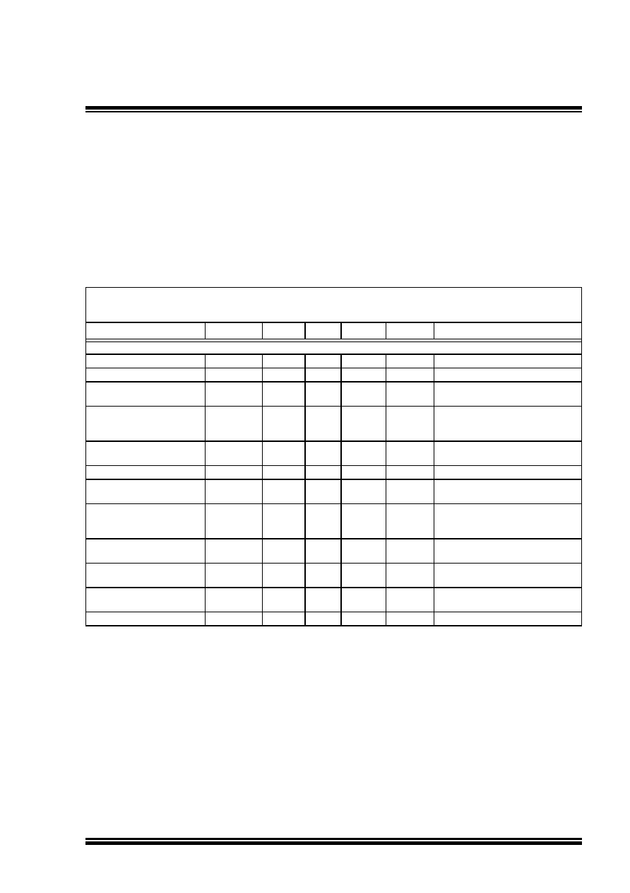
DC CHARACTERISTICS
Electrical Characteristics: Unless otherwise specified, all limits are established for VIN =VR +1, ILOAD = 100 A,
COUT =1F (X7R), CIN =1F (X7R), TA = +25°C.
Boldface type applies for junction temperatures, TJ (Note 6) of -40°C to +125°C.
Parameters
Sym
Min
Typ
Max
Units
Conditions
Input / Output Characteristics
Input Operating Voltage
VIN
2.3
—
6.0
V
Note 1
Input Quiescent Current
Iq
—1.6
4
A
IL =0mA, VIN =VR +1V
Maximum Output Current
IOUT_mA
250
200
—
mA
For VR ≥ 2.5V
For VR < 2.5V
Output Short Circuit Current
IOUT_SC
—
408
—
mA
VIN =VR +V, VOUT =GND,
Current (peak current) measured
10 ms after short is applied.
Output Voltage Regulation
VOUT
VR-3.0%
VR-2.0%
VR±0.4
%
VR+3.0%
VR+2.0%
V
Note 2
VOUT Temperature Coefficient
TCVOUT
—
50
—
ppm/°C
Note 3
Line Regulation
ΔVOUT/
(VOUTXΔVIN)
-1.0
±0.75
+1.0
%/V
(VR+1)V ≤ VIN ≤ 6V
Load Regulation
ΔVOUT/VOUT
-1.5
±1.0
+1.5
%IL = 0.1 mA to 250 mA for VR ≥ 2.5V
IL = 0.1 mA to 200 mA for VR < 2.5V
Note 4
Dropout Voltage
VR > 2.5V
VIN-VOUT
—
178
350
mV
IL = 250 mA, (Note 1, Note 5)
Dropout Voltage
VR < 2.5V
VIN-VOUT
—
150
350
mV
IL = 200 mA, (Note 1, Note 5)
Output Rise Time
TR
—
500
—
s
10% VR to 90% VR VIN = 0V to 6V,
RL =50Ω resistive
Output Noise
eN
—3
—
V/(Hz)1/2 IL = 100 mA, f = 1 kHz, COUT =1F
Note 1:
The minimum VIN must meet two conditions: VIN ≥ 2.3V and VIN ≥ (VR + 3.0%) +VDROPOUT.
2:
VR is the nominal regulator output voltage. For example: VR = 1.2V, 1.5V, 1.8V, 2.5V, 2.8V, 3.0V, 3.3V, 4.0V, 5.0V. The
input voltage (VIN =VR + 1.0V); IOUT = 100 A.
3:
TCVOUT = (VOUT-HIGH -VOUT-LOW) *106 / (VR * ΔTemperature), VOUT-HIGH = highest voltage measured over the
temperature range. VOUT-LOW = lowest voltage measured over the temperature range.
4:
Load regulation is measured at a constant junction temperature using low duty cycle pulse testing. Changes in output
voltage due to heating effects are determined using thermal regulation specification TCVOUT.
5:
Dropout voltage is defined as the input to output differential at which the output voltage drops 2% below its measured
value with a VR + 1V differential applied.
6:
The maximum allowable power dissipation is a function of ambient temperature, the maximum allowable junction
temperature and the thermal resistance from junction to air (i.e., TA, TJ, θJA). Exceeding the maximum allowable power
dissipation will cause the device operating junction temperature to exceed the maximum 150°C rating. Sustained
junction temperatures above 150°C can impact the device reliability.
7:
The junction temperature is approximated by soaking the device under test at an ambient temperature equal to the
desired Junction temperature. The test time is small enough such that the rise in the Junction temperature over the
ambient temperature is not significant.
相關(guān)PDF資料 |
PDF描述 |
|---|---|
| MCP1700T-3302ETT | Low Quiescent Current LDO |
| MCP1700T-5002EMB | Low Quiescent Current LDO |
| MCP1700T-5002ETO | Low Quiescent Current LDO |
| MCP6021R | Rail-to-Rail Input/Output, 10 MHz Op Amps |
| MCP604T-E/SL | QUAD OP-AMP, 4500 uV OFFSET-MAX, 2.8 MHz BAND WIDTH, PDSO14 |
相關(guān)代理商/技術(shù)參數(shù) |
參數(shù)描述 |
|---|---|
| MCP1700T-3502E/MB | 功能描述:低壓差穩(wěn)壓器 - LDO 250mA CMOS LDO Isupp 1uA 2% Vout Acc RoHS:否 制造商:Texas Instruments 最大輸入電壓:36 V 輸出電壓:1.4 V to 20.5 V 回動電壓(最大值):307 mV 輸出電流:1 A 負(fù)載調(diào)節(jié):0.3 % 輸出端數(shù)量: 輸出類型:Fixed 最大工作溫度:+ 125 C 安裝風(fēng)格:SMD/SMT 封裝 / 箱體:VQFN-20 |
| MCP1700T-3502E/TT | 功能描述:低壓差穩(wěn)壓器 - LDO 250mA CMOS LDO Isupp 1uA 2% Vout Acc RoHS:否 制造商:Texas Instruments 最大輸入電壓:36 V 輸出電壓:1.4 V to 20.5 V 回動電壓(最大值):307 mV 輸出電流:1 A 負(fù)載調(diào)節(jié):0.3 % 輸出端數(shù)量: 輸出類型:Fixed 最大工作溫度:+ 125 C 安裝風(fēng)格:SMD/SMT 封裝 / 箱體:VQFN-20 |
| MCP1700T-3602E/MB | 功能描述:低壓差穩(wěn)壓器 - LDO 250mA CMOS LDO Isupp 1uA 2% Vout Acc RoHS:否 制造商:Texas Instruments 最大輸入電壓:36 V 輸出電壓:1.4 V to 20.5 V 回動電壓(最大值):307 mV 輸出電流:1 A 負(fù)載調(diào)節(jié):0.3 % 輸出端數(shù)量: 輸出類型:Fixed 最大工作溫度:+ 125 C 安裝風(fēng)格:SMD/SMT 封裝 / 箱體:VQFN-20 |
| MCP1700T-3602E/TT | 功能描述:低壓差穩(wěn)壓器 - LDO 250mA CMOS LDO Isupp 1uA 2% Vout Acc RoHS:否 制造商:Texas Instruments 最大輸入電壓:36 V 輸出電壓:1.4 V to 20.5 V 回動電壓(最大值):307 mV 輸出電流:1 A 負(fù)載調(diào)節(jié):0.3 % 輸出端數(shù)量: 輸出類型:Fixed 最大工作溫度:+ 125 C 安裝風(fēng)格:SMD/SMT 封裝 / 箱體:VQFN-20 |
| MCP1700T-4002E/MB | 功能描述:低壓差穩(wěn)壓器 - LDO 250mA CMOS LDO Isupp 1uA 2% Vout Acc RoHS:否 制造商:Texas Instruments 最大輸入電壓:36 V 輸出電壓:1.4 V to 20.5 V 回動電壓(最大值):307 mV 輸出電流:1 A 負(fù)載調(diào)節(jié):0.3 % 輸出端數(shù)量: 輸出類型:Fixed 最大工作溫度:+ 125 C 安裝風(fēng)格:SMD/SMT 封裝 / 箱體:VQFN-20 |
發(fā)布緊急采購,3分鐘左右您將得到回復(fù)。