- 您現(xiàn)在的位置:買賣IC網(wǎng) > PDF目錄26805 > MC74HC10ANG (ON SEMICONDUCTOR) NAND GATE, PDIP14 PDF資料下載
參數(shù)資料
| 型號(hào): | MC74HC10ANG |
| 廠商: | ON SEMICONDUCTOR |
| 元件分類: | 門電路 |
| 英文描述: | NAND GATE, PDIP14 |
| 封裝: | LEAD FREE, PLASTIC, DIP-14 |
| 文件頁數(shù): | 2/8頁 |
| 文件大小: | 148K |
| 代理商: | MC74HC10ANG |
MC74HC10A
http://onsemi.com
2
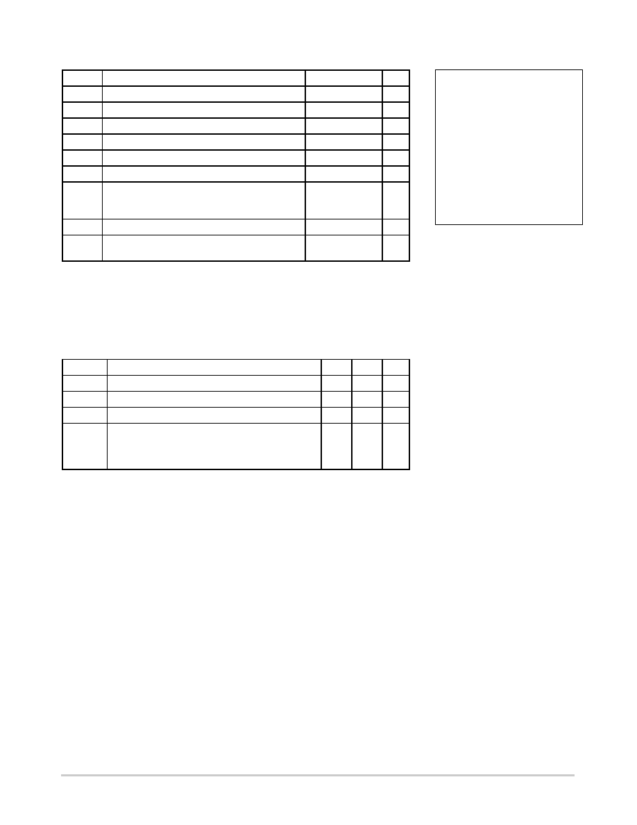
MAXIMUM RATINGS*
Symbol
Parameter
Value
Unit
VCC
DC Supply Voltage (Referenced to GND)
– 0.5 to + 7.0
V
Vin
DC Input Voltage (Referenced to GND)
– 0.5 to VCC + 0.5
V
Vout
DC Output Voltage (Referenced to GND)
– 0.5 to VCC + 0.5
V
Iin
DC Input Current, per Pin
± 20
mA
Iout
DC Output Current, per Pin
± 25
mA
ICC
DC Supply Current, VCC and GND Pins
± 50
mA
PD
Power Dissipation in Still Air
Plastic DIP
SOIC Package
TSSOP Package
750
500
450
mW
Tstg
Storage Temperature
– 65 to + 150
_C
TL
Lead Temperature, 1 mm from Case for 10 Seconds
(Plastic DIP, SOIC or TSSOP Package)
260
_C
Stresses exceeding Maximum Ratings may damage the device. Maximum Ratings are stress
ratings only. Functional operation above the Recommended Operating Conditions is not implied.
Extended exposure to stresses above the Recommended Operating Conditions may affect device
reliability.
Derating — Plastic DIP: – 10 mW/_C from 65_ to 125_C
SOIC Package: –7 mW/_C from 65_ to 125_C
TSSOP Package: 6.1 mW/_C from 65_ to 125_C
RECOMMENDED OPERATING CONDITIONS
Symbol
Parameter
Min
Max
Unit
VCC
DC Supply Voltage (Referenced to GND)
2.0
6.0
V
Vin, Vout
DC Input Voltage, Output Voltage (Referenced to GND)
0
VCC
V
TA
Operating Temperature, All Package Types
– 55
+ 125
_C
tr, tf
Input Rise and Fall Time
VCC = 2.0 V
(Figure 1)
VCC = 3.0 V
VCC = 4.5 V
VCC = 6.0 V
0
1000
600
500
400
ns
This device contains protection
circuitry to guard against damage
due to high static voltages or electric
fields. However, precautions must
be taken to avoid applications of any
voltage higher than maximum rated
voltages to this highimpedance cir-
cuit. For proper operation, Vin and
Vout should be constrained to the
range GND v (Vin or Vout) v VCC.
Unused inputs must always be
tied to an appropriate logic voltage
level (e.g., either GND or VCC).
Unused outputs must be left open.
相關(guān)PDF資料 |
PDF描述 |
|---|---|
| MC74HC10ADTR2G | NAND GATE, PDSO14 |
| MC74HC10ADR2G | NAND GATE, PDSO14 |
| MC74HC10ND | HC/UH SERIES, TRIPLE 3-INPUT NAND GATE, PDIP14 |
| MC74HC10DD | HC/UH SERIES, TRIPLE 3-INPUT NAND GATE, PDSO14 |
| MC74HC10DDR2 | HC/UH SERIES, TRIPLE 3-INPUT NAND GATE, PDSO14 |
相關(guān)代理商/技術(shù)參數(shù) |
參數(shù)描述 |
|---|---|
| MC74HC10DR2 | 制造商:ON Semiconductor 功能描述:NAND Gate 3-Element 3-IN CMOS 14-Pin SOIC T/R |
| MC74HC10F | 制造商:Rochester Electronics LLC 功能描述:- Bulk |
| MC74HC10FL2 | 制造商:Rochester Electronics LLC 功能描述:- Bulk |
| MC74HC10N | 制造商:Motorola Inc 功能描述: 制造商:ON SEM 功能描述: 制造商:ON Semiconductor 功能描述: |
| MC74HC10ND | 制造商:Motorola Inc 功能描述: |
發(fā)布緊急采購(gòu),3分鐘左右您將得到回復(fù)。