- 您現(xiàn)在的位置:買賣IC網(wǎng) > PDF目錄26805 > MC74HC04AFR2 (ON SEMICONDUCTOR) HC/UH SERIES, HEX 1-INPUT INVERT GATE, PDSO14 PDF資料下載
參數(shù)資料
| 型號(hào): | MC74HC04AFR2 |
| 廠商: | ON SEMICONDUCTOR |
| 元件分類: | 門電路 |
| 英文描述: | HC/UH SERIES, HEX 1-INPUT INVERT GATE, PDSO14 |
| 封裝: | EIAJ, SO-14 |
| 文件頁數(shù): | 2/9頁 |
| 文件大小: | 136K |
| 代理商: | MC74HC04AFR2 |
MC74HC04A
http://onsemi.com
2
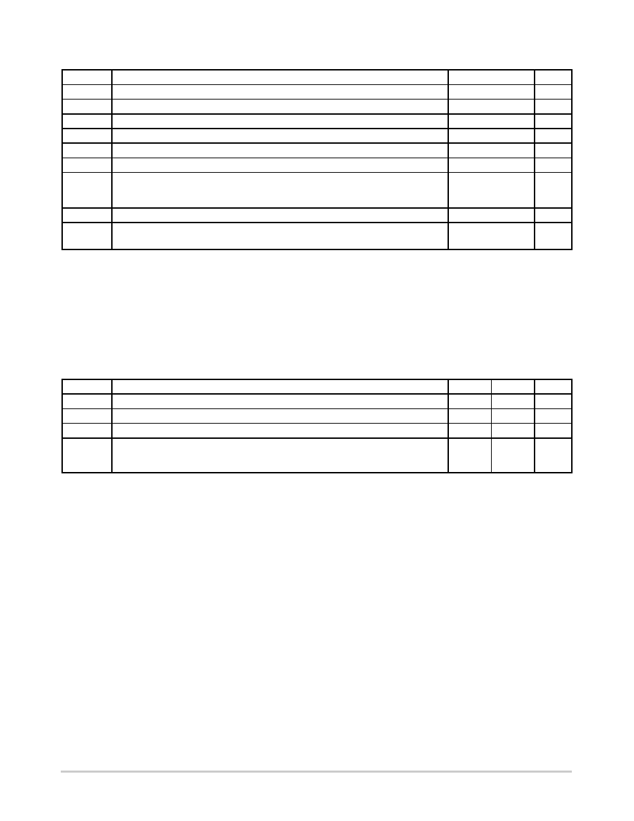
MAXIMUM RATINGS
Symbol
Parameter
Value
Unit
VCC
DC Supply Voltage (Referenced to GND)
– 0.5 to + 7.0
V
Vin
DC Input Voltage (Referenced to GND)
– 0.5 to VCC + 0.5
V
Vout
DC Output Voltage (Referenced to GND)
– 0.5 to VCC + 0.5
V
Iin
DC Input Current, per Pin
± 20
mA
Iout
DC Output Current, per Pin
± 25
mA
ICC
DC Supply Current, VCC and GND Pins
± 50
mA
PD
Power Dissipation in Still Air,
Plastic DIP
SOIC Package
TSSOP Package
750
500
450
mW
Tstg
Storage Temperature
– 65 to + 150
_C
TL
Lead Temperature, 1 mm from Case for 10 Seconds
Plastic DIP, SOIC or TSSOP Package
260
_C
Stresses exceeding Maximum Ratings may damage the device. Maximum Ratings are stress ratings only. Functional operation above the
Recommended Operating Conditions is not implied. Extended exposure to stresses above the Recommended Operating Conditions may affect
device reliability.
*This device contains protection circuitry to guard against damage due to high static voltages or electric fields. However, precautions must be
taken to avoid applications of any voltage higher than maximum rated voltages to this highimpedance circuit. For proper operation, Vin and
Vout should be constrained to the range GND v (Vin or Vout) v VCC. Unused inputs must always be tied to an appropriate logic voltage level
(e.g., either GND or VCC). Unused outputs must be left open.
Derating Plastic DIP: – 10 mW/_C from 65_ to 125_C
SOIC Package: – 7 mW/_C from 65_ to 125_C
TSSOP Package: 6.1 mW/_C from 65_ to 125_C
For high frequency or heavy load considerations, see Chapter 2 of the ON Semiconductor HighSpeed CMOS Data Book (DL129/D).
RECOMMENDED OPERATING CONDITIONS
Symbol
Parameter
Min
Max
Unit
VCC
DC Supply Voltage (Referenced to GND)
2.0
6.0
V
Vin, Vout
DC Input Voltage, Output Voltage (Referenced to GND)
0
VCC
V
TA
Operating Temperature, All Package Types
– 55
+ 125
_C
tr, tf
Input Rise and Fall Time
VCC = 2.0 V
(Figure 1)
VCC = 4.5 V
VCC = 6.0 V
0
1000
500
400
ns
相關(guān)PDF資料 |
PDF描述 |
|---|---|
| MC74HC04AND | HC/UH SERIES, HEX 1-INPUT INVERT GATE, PDIP14 |
| MC74HC04ADDR2 | HC/UH SERIES, HEX 1-INPUT INVERT GATE, PDSO14 |
| MC74HC107ND | HC/UH SERIES, DUAL NEGATIVE EDGE TRIGGERED J-K FLIP-FLOP, COMPLEMENTARY OUTPUT, PDIP14 |
| MC54HC107JD | HC/UH SERIES, DUAL NEGATIVE EDGE TRIGGERED J-K FLIP-FLOP, COMPLEMENTARY OUTPUT, CDIP14 |
| MC74HC10ANG | NAND GATE, PDIP14 |
相關(guān)代理商/技術(shù)參數(shù) |
參數(shù)描述 |
|---|---|
| MC74HC04AN | 功能描述:變換器 2-6V CMOS Hex RoHS:否 制造商:NXP Semiconductors 電路數(shù)量:6 邏輯系列:74ABT 邏輯類型:BiCMOS 高電平輸出電流:- 15 mA 低電平輸出電流:20 mA 傳播延遲時(shí)間:2.2 ns 電源電壓-最大:5.5 V 電源電壓-最小:4.5 V 最大工作溫度:+ 85 C 最小工作溫度:- 40 C 工作溫度范圍: 封裝 / 箱體:DIP-14 封裝:Tube |
| MC74HC04AND | 制造商:Motorola Inc 功能描述: |
| MC74HC04ANG | 功能描述:變換器 2-6V CMOS Hex RoHS:否 制造商:NXP Semiconductors 電路數(shù)量:6 邏輯系列:74ABT 邏輯類型:BiCMOS 高電平輸出電流:- 15 mA 低電平輸出電流:20 mA 傳播延遲時(shí)間:2.2 ns 電源電壓-最大:5.5 V 電源電壓-最小:4.5 V 最大工作溫度:+ 85 C 最小工作溫度:- 40 C 工作溫度范圍: 封裝 / 箱體:DIP-14 封裝:Tube |
| MC74HC04J | 制造商:Motorola Inc 功能描述:IC,LOGIC GATE,HEX INVERTER,HC-CMOS,DIP,14PIN,CERAMIC |
| MC74HC04M | 制造商:Fairchild Semiconductor Corporation 功能描述: |
發(fā)布緊急采購,3分鐘左右您將得到回復(fù)。