- 您現(xiàn)在的位置:買賣IC網(wǎng) > PDF目錄383561 > MC74ACT14NG (ON SEMICONDUCTOR) Hex Inverter Schmitt Trigger PDF資料下載
參數(shù)資料
| 型號: | MC74ACT14NG |
| 廠商: | ON SEMICONDUCTOR |
| 元件分類: | 通用總線功能 |
| 英文描述: | Hex Inverter Schmitt Trigger |
| 中文描述: | ACT SERIES, HEX 1-INPUT INVERT GATE, PDIP14 |
| 封裝: | LEAD FREE, PLASTIC, DIP-14 |
| 文件頁數(shù): | 2/9頁 |
| 文件大小: | 153K |
| 代理商: | MC74ACT14NG |
MC74AC14, MC74ACT14
http://onsemi.com
2
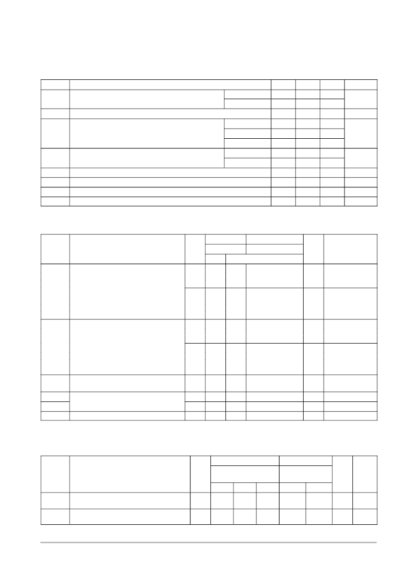
RECOMMENDED OPERATING CONDITIONS
Symbol
Parameter
Min
Typ
Max
Unit
V
CC
Supply Voltage
′
AC
′
ACT
2.0
4.5
5.0
5.0
6.0
5.5
V
V
in
, V
out
DC Input Voltage, Output Voltage (Ref. to GND)
0
V
CC
V
t
r
, t
f
Input Rise and Fall Time (Note 1)
′
AC Devices except Schmitt Inputs
V
CC
@ 3.0 V
V
CC
@ 4.5 V
V
CC
@ 5.5 V
V
CC
@ 4.5 V
V
CC
@ 5.5 V
150
40
ns/V
25
t
r
, t
f
Input Rise and Fall Time (Note 2)
′
ACT Devices except Schmitt Inputs
10
ns/V
8.0
T
J
T
A
I
OH
I
OL
Junction Temperature (PDIP)
140
°
C
°
C
Operating Ambient Temperature Range
40
25
85
Output Current
High
24
mA
Output Current
Low
24
mA
1. V
in
from 30% to 70% V
CC
; see individual Data Sheets for devices that differ from the typical input rise and fall times.
2. V
in
from 0.8 V to 2.0 V; see individual Data Sheets for devices that differ from the typical input rise and fall times.
DC CHARACTERISTICS
Symbol
Parameter
V
CC
(V)
74AC
74AC
Unit
Conditions
T
A
= +25
°
C
Typ
T
A
=
40
°
C to +85
°
C
Guaranteed Limits
V
OH
Minimum High Level Output Voltage
3.0
4.5
5.5
2.99
4.49
5.49
2.9
4.4
5.4
2.9
4.4
5.4
I
OUT
=
50 A
V
V
*V
IN
= V
IL
or V
IH
3.0
4.5
5.5
2.56
3.86
4.86
2.46
3.76
4.76
12 mA
24 mA
24 mA
I
OH
V
OL
Maximum Low Level Output Voltage
3.0
4.5
5.5
0.002
0.001
0.001
0.1
0.1
0.1
0.1
0.1
0.1
I
OUT
= 50 A
V
V
*V
IN
= V
IL
or V
IH
3.0
4.5
5.5
0.36
0.36
0.36
0.44
0.44
0.44
12 mA
24 mA
24 mA
I
OL
I
IN
Maximum Input Leakage Current
5.5
±
0.1
±
1.0
A
V
I
= V
CC
, GND
I
OLD
I
OHD
I
CC
Minimum Dynamic Output Current
5.5
75
mA
V
OLD
= 1.65 V Max
V
OHD
= 3.85 V Min
V
IN
= V
CC
or GND
5.5
75
mA
Maximum Quiescent Supply Current
*All outputs loaded; thresholds on input associated with output under test.
Maximum test duration 2.0 ms, one output loaded at a time.
NOTE:
I
IN
and I
CC
@ 3.0 V are guaranteed to be less than or equal to the respective limit @ 5.5 V V
CC
.
5.5
4.0
40
A
AC CHARACTERISTICS
(For Figures and Waveforms
See Section 3 of the ON Semiconductor FACT Data Book, DL138/D)
Symbol
Parameter
V
CC
*
(V)
74AC
74AC
Unit
Figure
No.
T
A
= +25
°
C C
L
= 50 pF
T
A
=
40
°
C to
+85
°
C C
L
= 50 pF
Min
Typ
Max
Min
Max
t
PLH
Propagation Delay
3.3
5.0
3.3
5.0
1.5
1.5
1.5
1.5
9.5
7.0
7.5
6.0
13.5
10.0
11.5
8.5
1.5
1.5
1.5
1.5
15.0
11.0
13.0
9.5
ns
3
5
t
PHL
Propagation Delay
ns
3
5
*Voltage Range 3.3 V is 3.3 V
±
0.3 V. Voltage Range 5.0 V is 5.0 V
±
0.5 V.
相關(guān)PDF資料 |
PDF描述 |
|---|---|
| MC74AC151DR2 | 1−of−8 Decoder/Demultiplexer |
| MC74AC151DT | 1−of−8 Decoder/Demultiplexer |
| MC74AC151DTR2 | 1−of−8 Decoder/Demultiplexer |
| MC74AC151M | 1−of−8 Decoder/Demultiplexer |
| MC74ACT151 | 1−of−8 Decoder/Demultiplexer |
相關(guān)代理商/技術(shù)參數(shù) |
參數(shù)描述 |
|---|---|
| MC74ACT14NG | 制造商:ON Semiconductor 功能描述:Gate / Inverter Logic IC |
| MC74ACT151 | 制造商:ONSEMI 制造商全稱:ON Semiconductor 功能描述:1−of−8 Decoder/Demultiplexer |
| MC74ACT151D | 制造商:Rochester Electronics LLC 功能描述:- Bulk 制造商:Motorola Inc 功能描述: 制造商:ON Semiconductor 功能描述: |
| MC74ACT151DR2 | 制造商:Rochester Electronics LLC 功能描述:- Bulk 制造商:Motorola Inc 功能描述: 制造商:ON Semiconductor 功能描述: 制造商:MOTOROLA 功能描述: |
| MC74ACT151DT | 制造商:ONSEMI 制造商全稱:ON Semiconductor 功能描述:1−of−8 Decoder/Demultiplexer |
發(fā)布緊急采購,3分鐘左右您將得到回復(fù)。