- 您現(xiàn)在的位置:買賣IC網(wǎng) > PDF目錄45231 > MC68HC11KS1CFN2 (MOTOROLA INC) 8-BIT, MROM, 2 MHz, MICROCONTROLLER, PQCC68 PDF資料下載
參數(shù)資料
| 型號: | MC68HC11KS1CFN2 |
| 廠商: | MOTOROLA INC |
| 元件分類: | 微控制器/微處理器 |
| 英文描述: | 8-BIT, MROM, 2 MHz, MICROCONTROLLER, PQCC68 |
| 封裝: | PLASTIC, LCC-68 |
| 文件頁數(shù): | 308/341頁 |
| 文件大?。?/td> | 4256K |
| 代理商: | MC68HC11KS1CFN2 |
第1頁第2頁第3頁第4頁第5頁第6頁第7頁第8頁第9頁第10頁第11頁第12頁第13頁第14頁第15頁第16頁第17頁第18頁第19頁第20頁第21頁第22頁第23頁第24頁第25頁第26頁第27頁第28頁第29頁第30頁第31頁第32頁第33頁第34頁第35頁第36頁第37頁第38頁第39頁第40頁第41頁第42頁第43頁第44頁第45頁第46頁第47頁第48頁第49頁第50頁第51頁第52頁第53頁第54頁第55頁第56頁第57頁第58頁第59頁第60頁第61頁第62頁第63頁第64頁第65頁第66頁第67頁第68頁第69頁第70頁第71頁第72頁第73頁第74頁第75頁第76頁第77頁第78頁第79頁第80頁第81頁第82頁第83頁第84頁第85頁第86頁第87頁第88頁第89頁第90頁第91頁第92頁第93頁第94頁第95頁第96頁第97頁第98頁第99頁第100頁第101頁第102頁第103頁第104頁第105頁第106頁第107頁第108頁第109頁第110頁第111頁第112頁第113頁第114頁第115頁第116頁第117頁第118頁第119頁第120頁第121頁第122頁第123頁第124頁第125頁第126頁第127頁第128頁第129頁第130頁第131頁第132頁第133頁第134頁第135頁第136頁第137頁第138頁第139頁第140頁第141頁第142頁第143頁第144頁第145頁第146頁第147頁第148頁第149頁第150頁第151頁第152頁第153頁第154頁第155頁第156頁第157頁第158頁第159頁第160頁第161頁第162頁第163頁第164頁第165頁第166頁第167頁第168頁第169頁第170頁第171頁第172頁第173頁第174頁第175頁第176頁第177頁第178頁第179頁第180頁第181頁第182頁第183頁第184頁第185頁第186頁第187頁第188頁第189頁第190頁第191頁第192頁第193頁第194頁第195頁第196頁第197頁第198頁第199頁第200頁第201頁第202頁第203頁第204頁第205頁第206頁第207頁第208頁第209頁第210頁第211頁第212頁第213頁第214頁第215頁第216頁第217頁第218頁第219頁第220頁第221頁第222頁第223頁第224頁第225頁第226頁第227頁第228頁第229頁第230頁第231頁第232頁第233頁第234頁第235頁第236頁第237頁第238頁第239頁第240頁第241頁第242頁第243頁第244頁第245頁第246頁第247頁第248頁第249頁第250頁第251頁第252頁第253頁第254頁第255頁第256頁第257頁第258頁第259頁第260頁第261頁第262頁第263頁第264頁第265頁第266頁第267頁第268頁第269頁第270頁第271頁第272頁第273頁第274頁第275頁第276頁第277頁第278頁第279頁第280頁第281頁第282頁第283頁第284頁第285頁第286頁第287頁第288頁第289頁第290頁第291頁第292頁第293頁第294頁第295頁第296頁第297頁第298頁第299頁第300頁第301頁第302頁第303頁第304頁第305頁第306頁第307頁當(dāng)前第308頁第309頁第310頁第311頁第312頁第313頁第314頁第315頁第316頁第317頁第318頁第319頁第320頁第321頁第322頁第323頁第324頁第325頁第326頁第327頁第328頁第329頁第330頁第331頁第332頁第333頁第334頁第335頁第336頁第337頁第338頁第339頁第340頁第341頁
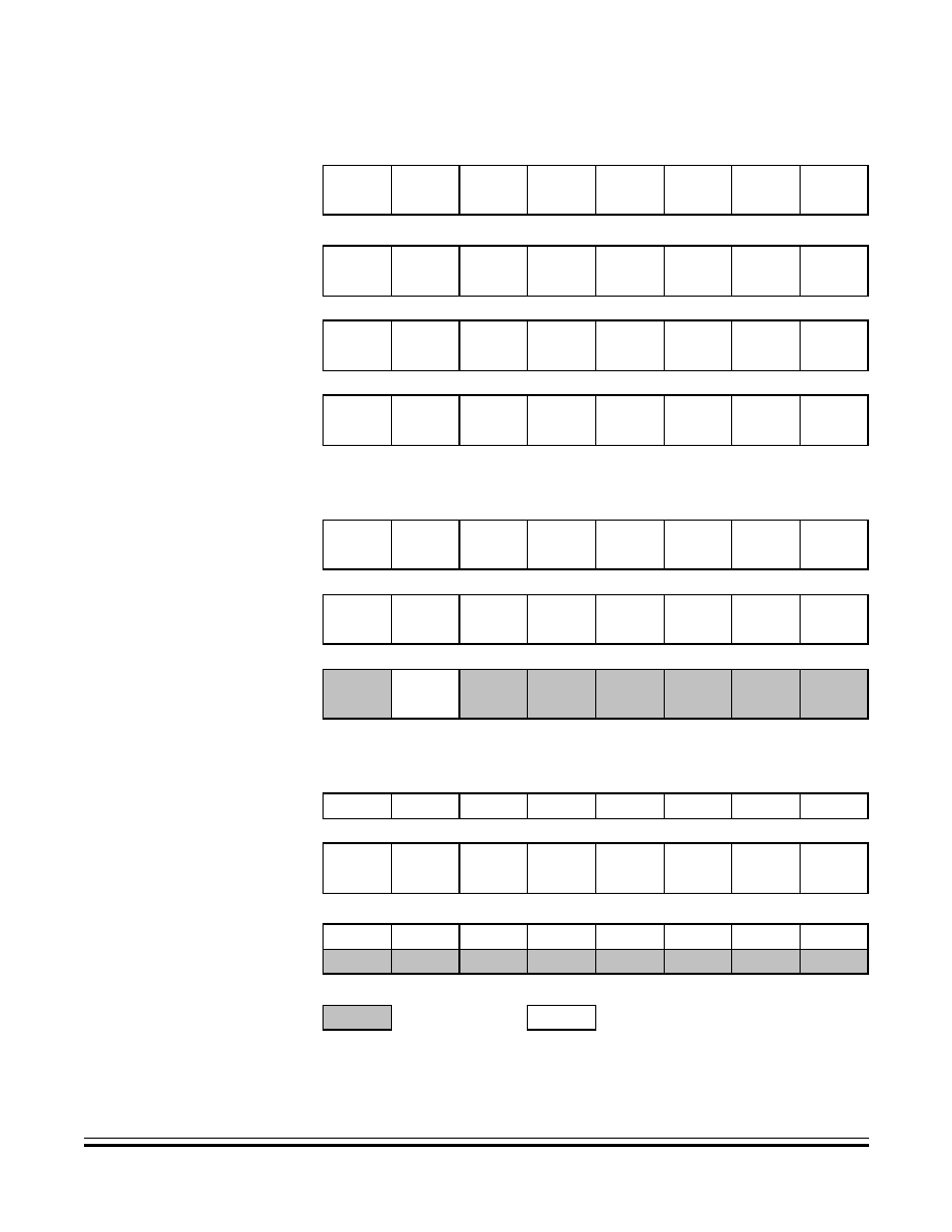
Operating Modes and On-Chip Memory
Control Registers
M68HC11K Family
Technical Data
MOTOROLA
Operating Modes and On-Chip Memory
69
$0028
Serial Peripheral
Control Register
(SPCR)
Read:
SPIE
SPE
DWOM
MSTR
CPOL
CPHA
SPR1
SPR0
Write:
Reset:
00
01
U
$0029
Serial Peripheral Status
Register (SPSR)
Read:
SPIF
WCOL
0
MODF
00
Write:
Reset:
00
$002A
Serial Peripheral Data
Register (SPDR)
Read:
Bit 7Bit 6
Bit 5Bit 4
Bit 3Bit 2
Bit 1Bit 0
Write:
Reset:
Undefined after reset
$002B
EPROM Programming
Control Register
(EPROG)(1)
Read:
R
0
ELAT
EXCOL
EXROW
0
EPGM
Write:
Reset:
00
1. Present only in EPROM (711) devices
$002C
Port Pullup Assignment
Register (PPAR)
Read:
0
HPPUE
GPPUE
FPPUE
BPPUE
Write:
Reset:
00
11
$002D
Port G Assignment
Register (PGAR)
Read:
0
PGAR5
PGAR4
PGAR3
PGAR2
PGAR1
PGAR0
Write:
Reset:
00
$002E
System Configuration
Options 3 Register
(OPT3)(2)
Read:
SM
Write:
Reset:
00
2. Not available on M68HC11K4 devices
$002F
Reserved
R
$0030
Analog-to-Digital
Control/Status Register
(ADCTL)
Read:
CCF
0
SCAN
MULT
CD
CC
CB
CA
Write:
Reset:
0
UU
U
$0031
Analog-to-Digital
Results Register 1
(ADR1)
Read:
Bit 7
Bit 6
Bit 5
Bit 4
Bit 3
Bit 2
Bit 1
Bit 0
Write:
Reset:
Undefined after reset
Addr.
Register Name
Bit 7
6
5
4
3
2
1
Bit 0
= Unimplemented
R
= Reserved
U = Undefined
Figure 4-1. Register and Control Bit Assignments (Sheet 5 of 11)
相關(guān)PDF資料 |
PDF描述 |
|---|---|
| MC68HC711KS2CFN2 | 8-BIT, OTPROM, 2 MHz, MICROCONTROLLER, PQCC68 |
| MC68HC711K4CFU2 | 8-BIT, OTPROM, 2 MHz, MICROCONTROLLER, PQFP80 |
| MC68HC711KS2VFN4 | 8-BIT, OTPROM, 4 MHz, MICROCONTROLLER, PQCC68 |
| MC68HC11KS1MFN4 | 8-BIT, MROM, 4 MHz, MICROCONTROLLER, PQCC68 |
| MC68HC11KS2MFN4 | 8-BIT, MROM, 4 MHz, MICROCONTROLLER, PQCC68 |
相關(guān)代理商/技術(shù)參數(shù) |
參數(shù)描述 |
|---|---|
| MC68HC11KS2 | 制造商:FREESCALE 制造商全稱:Freescale Semiconductor, Inc 功能描述:HCMOS Microcontroller Unit |
| MC68HC11KTS | 制造商:MOTOROLA 制造商全稱:Motorola, Inc 功能描述:8-Bit Microcontroller |
| MC68HC11KW1 | 制造商:FREESCALE 制造商全稱:Freescale Semiconductor, Inc 功能描述:High-density complementary metal oxide semiconductor (HCMOS) microcontroller unit |
| MC68HC11L0 | 制造商:MOTOROLA 制造商全稱:Motorola, Inc 功能描述:CONFIG Register Programming for EEPROM-based M68HC11 Microcontrollers |
| MC68HC11L0CFN2 | 制造商:FREESCALE 制造商全稱:Freescale Semiconductor, Inc 功能描述:HCMOS MICROCONTROLLER UNIT |
發(fā)布緊急采購,3分鐘左右您將得到回復(fù)。