- 您現(xiàn)在的位置:買賣IC網(wǎng) > PDF目錄45224 > MC68HC08GR32AVFU (FREESCALE SEMICONDUCTOR INC) 8-BIT, MROM, 8 MHz, MICROCONTROLLER, PQFP64 PDF資料下載
參數(shù)資料
| 型號(hào): | MC68HC08GR32AVFU |
| 廠商: | FREESCALE SEMICONDUCTOR INC |
| 元件分類: | 微控制器/微處理器 |
| 英文描述: | 8-BIT, MROM, 8 MHz, MICROCONTROLLER, PQFP64 |
| 封裝: | 14 X 14 MM, QFP-64 |
| 文件頁數(shù): | 143/286頁 |
| 文件大?。?/td> | 2074K |
| 代理商: | MC68HC08GR32AVFU |
第1頁第2頁第3頁第4頁第5頁第6頁第7頁第8頁第9頁第10頁第11頁第12頁第13頁第14頁第15頁第16頁第17頁第18頁第19頁第20頁第21頁第22頁第23頁第24頁第25頁第26頁第27頁第28頁第29頁第30頁第31頁第32頁第33頁第34頁第35頁第36頁第37頁第38頁第39頁第40頁第41頁第42頁第43頁第44頁第45頁第46頁第47頁第48頁第49頁第50頁第51頁第52頁第53頁第54頁第55頁第56頁第57頁第58頁第59頁第60頁第61頁第62頁第63頁第64頁第65頁第66頁第67頁第68頁第69頁第70頁第71頁第72頁第73頁第74頁第75頁第76頁第77頁第78頁第79頁第80頁第81頁第82頁第83頁第84頁第85頁第86頁第87頁第88頁第89頁第90頁第91頁第92頁第93頁第94頁第95頁第96頁第97頁第98頁第99頁第100頁第101頁第102頁第103頁第104頁第105頁第106頁第107頁第108頁第109頁第110頁第111頁第112頁第113頁第114頁第115頁第116頁第117頁第118頁第119頁第120頁第121頁第122頁第123頁第124頁第125頁第126頁第127頁第128頁第129頁第130頁第131頁第132頁第133頁第134頁第135頁第136頁第137頁第138頁第139頁第140頁第141頁第142頁當(dāng)前第143頁第144頁第145頁第146頁第147頁第148頁第149頁第150頁第151頁第152頁第153頁第154頁第155頁第156頁第157頁第158頁第159頁第160頁第161頁第162頁第163頁第164頁第165頁第166頁第167頁第168頁第169頁第170頁第171頁第172頁第173頁第174頁第175頁第176頁第177頁第178頁第179頁第180頁第181頁第182頁第183頁第184頁第185頁第186頁第187頁第188頁第189頁第190頁第191頁第192頁第193頁第194頁第195頁第196頁第197頁第198頁第199頁第200頁第201頁第202頁第203頁第204頁第205頁第206頁第207頁第208頁第209頁第210頁第211頁第212頁第213頁第214頁第215頁第216頁第217頁第218頁第219頁第220頁第221頁第222頁第223頁第224頁第225頁第226頁第227頁第228頁第229頁第230頁第231頁第232頁第233頁第234頁第235頁第236頁第237頁第238頁第239頁第240頁第241頁第242頁第243頁第244頁第245頁第246頁第247頁第248頁第249頁第250頁第251頁第252頁第253頁第254頁第255頁第256頁第257頁第258頁第259頁第260頁第261頁第262頁第263頁第264頁第265頁第266頁第267頁第268頁第269頁第270頁第271頁第272頁第273頁第274頁第275頁第276頁第277頁第278頁第279頁第280頁第281頁第282頁第283頁第284頁第285頁第286頁
Functional Description
MC68HC08GR32A MC68HC08GR16A Data Sheet, Rev. 0
Freescale Semiconductor
227
18.3.2 Input Capture
An input capture function has three basic parts: edge select logic, an input capture latch, and a 16-bit
counter. Two 8-bit registers, which make up the 16-bit input capture register, are used to latch the value
of the free-running counter after the corresponding input capture edge detector senses a defined
transition. The polarity of the active edge is programmable. The level transition which triggers the counter
transfer is defined by the corresponding input edge bits (ELSxB and ELSxA in T2SC0 through T2SC5
control registers with x referring to the active channel number). When an active edge occurs on the pin of
an input capture channel, the TIM2 latches the contents of the TIM2 counter into the TIM2 channel
registers, T2CHxH:T2CHxL. Input captures can generate TIM2 CPU interrupt requests. Software can
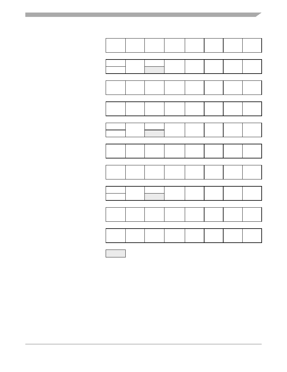
$0458
TIM2 Channel 2 Register Low
(T2CH2L)
Read:
Bit 7
6
5
4
3
2
1
Bit 0
Write:
Reset:
Indeterminate after reset
$0459
TIM2 Channel 3 Status and Con-
trol Register (T2SC3)
Read:
CH3F
CH3IE
0
MS3A
ELS3B
ELS3A
TOV3
CH3MAX
Write:
0
Reset:
0
$045A
TIM2 Channel 3 Register High
(T2CH3H)
Read:
Bit 15
14
13
12
11
10
9
Bit 8
Write:
Reset:
Indeterminate after reset
$045B
TIM2 Channel 3 Register Low
(T2CH3L
Read:
Bit 7
6
5
4
3
2
1
Bit 0
Write:
Reset:
Indeterminate after reset
$045C
TIM2 Channel 4 Status and Con-
trol Register (T2SC4)
Read:
CH4F
CH4IE
0
MS4A
ELS4B
ELS4A
TOV4
CH4MAX
Write:
0
Reset:
0
$045D
TIM2 Channel 4 Register High
(T2CH4H)
Read:
Bit 15
14
13
12
11
10
9
Bit 8
Write:
Reset:
Indeterminate after reset
$045E
TIM2 Channel 4 Register Low
(T2CH4L)
Read:
Bit 7
6
5
4
3
2
1
Bit 0
Write:
Reset:
Indeterminate after reset
$045F
TIM2 Channel 5 Status and Con-
trol Register (T2SC5)
Read:
CH5F
CH5IE
0
MS5A
ELS5B
ELS5A
TOV5
CH5MAX
Write:
0
Reset:
0
$0460
TIM2 Channel 5 Register High
(T2CH5H)
Read:
Bit 15
14
13
12
11
10
9
Bit 8
Write:
Reset:
Indeterminate after reset
$0461
TIM2 Channel 5 Register Low
(T2CH5L)
Read:
Bit 7
6
5
4
3
2
1
Bit 0
Write:
Reset:
Indeterminate after reset
Addr.
Register Name
Bit 7
6
5
4
3
2
1
Bit 0
= Unimplemented
Figure 18-3. TIM2 I/O Register Summary (Sheet 2 of 2)
相關(guān)PDF資料 |
PDF描述 |
|---|---|
| MC68HC08GR32AVFA | 8-BIT, MROM, 8 MHz, MICROCONTROLLER, PQFP48 |
| MC68HC08GZ32VFJ | 8-BIT, MROM, 8 MHz, MICROCONTROLLER, PQFP32 |
| MC68HC08GZ32VFJE | 8-BIT, MROM, 8 MHz, MICROCONTROLLER, PQFP32 |
| MC68HC08GZ32MFJ | 8-BIT, MROM, 8 MHz, MICROCONTROLLER, PQFP32 |
| MC68HC08GZ32CFJ | 8-BIT, MROM, 8 MHz, MICROCONTROLLER, PQFP32 |
相關(guān)代理商/技術(shù)參數(shù) |
參數(shù)描述 |
|---|---|
| MC68HC08GT16 | 制造商:FREESCALE 制造商全稱:Freescale Semiconductor, Inc 功能描述:Microcontrollers |
| MC68HC08GZ32 | 制造商:FREESCALE 制造商全稱:Freescale Semiconductor, Inc 功能描述:Microcontrollers |
| MC68HC08GZ32CFA | 制造商:FREESCALE 制造商全稱:Freescale Semiconductor, Inc 功能描述:Microcontrollers |
| MC68HC08GZ32CFJ | 制造商:FREESCALE 制造商全稱:Freescale Semiconductor, Inc 功能描述:Microcontrollers |
| MC68HC08GZ32CFU | 制造商:FREESCALE 制造商全稱:Freescale Semiconductor, Inc 功能描述:Microcontrollers |
發(fā)布緊急采購,3分鐘左右您將得到回復(fù)。