- 您現(xiàn)在的位置:買賣IC網(wǎng) > PDF目錄45235 > MC68HC05B6FNE (FREESCALE SEMICONDUCTOR INC) 8-BIT, MROM, 2.1 MHz, MICROCONTROLLER, PQCC52 PDF資料下載
參數(shù)資料
| 型號: | MC68HC05B6FNE |
| 廠商: | FREESCALE SEMICONDUCTOR INC |
| 元件分類: | 微控制器/微處理器 |
| 英文描述: | 8-BIT, MROM, 2.1 MHz, MICROCONTROLLER, PQCC52 |
| 封裝: | PLASTIC, LCC-52 |
| 文件頁數(shù): | 62/302頁 |
| 文件大?。?/td> | 3940K |
| 代理商: | MC68HC05B6FNE |
第1頁第2頁第3頁第4頁第5頁第6頁第7頁第8頁第9頁第10頁第11頁第12頁第13頁第14頁第15頁第16頁第17頁第18頁第19頁第20頁第21頁第22頁第23頁第24頁第25頁第26頁第27頁第28頁第29頁第30頁第31頁第32頁第33頁第34頁第35頁第36頁第37頁第38頁第39頁第40頁第41頁第42頁第43頁第44頁第45頁第46頁第47頁第48頁第49頁第50頁第51頁第52頁第53頁第54頁第55頁第56頁第57頁第58頁第59頁第60頁第61頁當(dāng)前第62頁第63頁第64頁第65頁第66頁第67頁第68頁第69頁第70頁第71頁第72頁第73頁第74頁第75頁第76頁第77頁第78頁第79頁第80頁第81頁第82頁第83頁第84頁第85頁第86頁第87頁第88頁第89頁第90頁第91頁第92頁第93頁第94頁第95頁第96頁第97頁第98頁第99頁第100頁第101頁第102頁第103頁第104頁第105頁第106頁第107頁第108頁第109頁第110頁第111頁第112頁第113頁第114頁第115頁第116頁第117頁第118頁第119頁第120頁第121頁第122頁第123頁第124頁第125頁第126頁第127頁第128頁第129頁第130頁第131頁第132頁第133頁第134頁第135頁第136頁第137頁第138頁第139頁第140頁第141頁第142頁第143頁第144頁第145頁第146頁第147頁第148頁第149頁第150頁第151頁第152頁第153頁第154頁第155頁第156頁第157頁第158頁第159頁第160頁第161頁第162頁第163頁第164頁第165頁第166頁第167頁第168頁第169頁第170頁第171頁第172頁第173頁第174頁第175頁第176頁第177頁第178頁第179頁第180頁第181頁第182頁第183頁第184頁第185頁第186頁第187頁第188頁第189頁第190頁第191頁第192頁第193頁第194頁第195頁第196頁第197頁第198頁第199頁第200頁第201頁第202頁第203頁第204頁第205頁第206頁第207頁第208頁第209頁第210頁第211頁第212頁第213頁第214頁第215頁第216頁第217頁第218頁第219頁第220頁第221頁第222頁第223頁第224頁第225頁第226頁第227頁第228頁第229頁第230頁第231頁第232頁第233頁第234頁第235頁第236頁第237頁第238頁第239頁第240頁第241頁第242頁第243頁第244頁第245頁第246頁第247頁第248頁第249頁第250頁第251頁第252頁第253頁第254頁第255頁第256頁第257頁第258頁第259頁第260頁第261頁第262頁第263頁第264頁第265頁第266頁第267頁第268頁第269頁第270頁第271頁第272頁第273頁第274頁第275頁第276頁第277頁第278頁第279頁第280頁第281頁第282頁第283頁第284頁第285頁第286頁第287頁第288頁第289頁第290頁第291頁第292頁第293頁第294頁第295頁第296頁第297頁第298頁第299頁第300頁第301頁第302頁
Freescale
A-4
MC68HC05B6
Rev. 4.1
MC68HC05B4
14
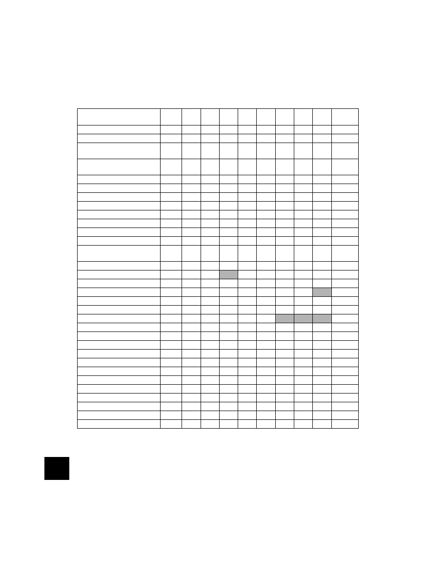
Table A-2 Register outline
Register name
Address bit 7
bit 6
bit 5
bit 4
bit 3
bit 2
bit 1
bit 0
State on
reset
Port A data (PORTA)
$0000
Undefined
Port B data (PORTB)
$0001
Undefined
Port C data (PORTC)
$0002
PC2/
ECLK
Undefined
Port D data (PORTD)
$0003
PD7/
AN7
PD6/
AN6
PD5/
AN5
PD4/
AN4
PD3/
AN3
PD2/
AN2
PD1/
AN1
PD0/
AN0
Undefined
Port A data direction (DDRA)
$0004
0000 0000
Port B data direction (DDRB)
$0005
0000 0000
Port C data direction (DDRC)
$0006
0000 0000
ECLK control
$0007
0
ECLK
0
0000 0000
A/D data (ADDATA)
$0008
0000 0000
A/D status/control (ADSTAT)
$0009 COCO ADRC ADON
0
CH3
CH2
CH1
CH0 0000 0000
Pulse length modulation A (PLMA)
$000A
0000 0000
Pulse length modulation B (PLMB)
$000B
0000 0000
Miscellaneous
$000C POR(1) INTP
INTN
INTE
SFA
SFB
SM
WDOG
(2)
?001 000?
SCI baud rate (BAUD)
$000D
SPC1 SPC0 SCT1 SCT0 SCT0 SCR2 SCR1 SCR0 00uu uuuu
SCI control 1 (SCCR1)
$000E
R8
T8
M
WAKE CPOL CPHA LBCL uuuu uuuu
SCI control 2 (SCCR2)
$000F
TIE
TCIE
RIE
ILIE
TE
RE
RWU
SBK 0000 0000
SCI status (SCSR)
$0010
TDRE
TC
RDRF IDLE
OR
NF
FE
1100 000u
SCI data (SCDR)
$0011
0000 0000
Timer control (TCR)
$0012
ICIE
OCIE
TOIE FOLV2 FOLV1 OLV2 IEDG1 OLVL1 0000 00u0
Timer status (TSR)
$0013
ICF1
OCF1
TOF
ICF2
OCF2
uuuu uuuu
Input capture high 1
$0014
Undefined
Input capture low 1
$0015
Undefined
Output compare high 1
$0016
Undefined
Output compare low 1
$0017
Undefined
Timer counter high
$0018
1111 1111
Timer counter low
$0019
1111 1100
Alternate counter high
$001A
1111 1111
Alternate counter low
$001B
1111 1100
Input capture high 2
$001C
Undefined
Input capture low 2
$001D
Undefined
Output compare high 2
$001E
Undefined
Output compare low 2
$001F
Undefined
(1) This bit is set each time there is a power-on reset.
(2) The state of the WDOG bit after reset is dependent upon the mask option selected; 1=watchdog enabled, 0=watchdog disabled.
相關(guān)PDF資料 |
PDF描述 |
|---|---|
| MC68HC05B4VFN | 8-BIT, MROM, 2.1 MHz, MICROCONTROLLER, PQCC52 |
| MC68HC05B6CFU | 8-BIT, MROM, 2.1 MHz, MICROCONTROLLER, PQFP64 |
| MC68HC05B8MB | 8-BIT, MROM, 2.1 MHz, MICROCONTROLLER, PDIP56 |
| MC68HC05B8MFN | 8-BIT, MROM, 2.1 MHz, MICROCONTROLLER, PQCC52 |
| MC68HC705B16NVFN | 8-BIT, OTPROM, 2.1 MHz, MICROCONTROLLER, PQCC52 |
相關(guān)代理商/技術(shù)參數(shù) |
參數(shù)描述 |
|---|---|
| MC68HC05B8 | 制造商:FREESCALE 制造商全稱:Freescale Semiconductor, Inc 功能描述:Microcontrollers |
| MC68HC05BD3 | 制造商:FREESCALE 制造商全稱:Freescale Semiconductor, Inc 功能描述:High-density complementary metal oxide semiconductor (HCMOS) microcontroller unit |
| MC68HC05BD5 | 制造商:FREESCALE 制造商全稱:Freescale Semiconductor, Inc 功能描述:High-density complementary metal oxide semiconductor (HCMOS) microcontroller unit |
| MC68HC05C0CP | 制造商:Motorola Inc 功能描述: |
| MC68HC05C12 | 制造商:FREESCALE 制造商全稱:Freescale Semiconductor, Inc 功能描述:HCMOS MICROCONTROLLER UNITS |
發(fā)布緊急采購,3分鐘左右您將得到回復(fù)。