- 您現(xiàn)在的位置:買賣IC網(wǎng) > PDF目錄359140 > MC68H08GT16 (飛思卡爾半導(dǎo)體(中國)有限公司) Microcontrollers(微控制器) PDF資料下載
參數(shù)資料
| 型號(hào): | MC68H08GT16 |
| 廠商: | 飛思卡爾半導(dǎo)體(中國)有限公司 |
| 英文描述: | Microcontrollers(微控制器) |
| 中文描述: | 微控制器(微控制器) |
| 文件頁數(shù): | 46/292頁 |
| 文件大?。?/td> | 2134K |
| 代理商: | MC68H08GT16 |
第1頁第2頁第3頁第4頁第5頁第6頁第7頁第8頁第9頁第10頁第11頁第12頁第13頁第14頁第15頁第16頁第17頁第18頁第19頁第20頁第21頁第22頁第23頁第24頁第25頁第26頁第27頁第28頁第29頁第30頁第31頁第32頁第33頁第34頁第35頁第36頁第37頁第38頁第39頁第40頁第41頁第42頁第43頁第44頁第45頁當(dāng)前第46頁第47頁第48頁第49頁第50頁第51頁第52頁第53頁第54頁第55頁第56頁第57頁第58頁第59頁第60頁第61頁第62頁第63頁第64頁第65頁第66頁第67頁第68頁第69頁第70頁第71頁第72頁第73頁第74頁第75頁第76頁第77頁第78頁第79頁第80頁第81頁第82頁第83頁第84頁第85頁第86頁第87頁第88頁第89頁第90頁第91頁第92頁第93頁第94頁第95頁第96頁第97頁第98頁第99頁第100頁第101頁第102頁第103頁第104頁第105頁第106頁第107頁第108頁第109頁第110頁第111頁第112頁第113頁第114頁第115頁第116頁第117頁第118頁第119頁第120頁第121頁第122頁第123頁第124頁第125頁第126頁第127頁第128頁第129頁第130頁第131頁第132頁第133頁第134頁第135頁第136頁第137頁第138頁第139頁第140頁第141頁第142頁第143頁第144頁第145頁第146頁第147頁第148頁第149頁第150頁第151頁第152頁第153頁第154頁第155頁第156頁第157頁第158頁第159頁第160頁第161頁第162頁第163頁第164頁第165頁第166頁第167頁第168頁第169頁第170頁第171頁第172頁第173頁第174頁第175頁第176頁第177頁第178頁第179頁第180頁第181頁第182頁第183頁第184頁第185頁第186頁第187頁第188頁第189頁第190頁第191頁第192頁第193頁第194頁第195頁第196頁第197頁第198頁第199頁第200頁第201頁第202頁第203頁第204頁第205頁第206頁第207頁第208頁第209頁第210頁第211頁第212頁第213頁第214頁第215頁第216頁第217頁第218頁第219頁第220頁第221頁第222頁第223頁第224頁第225頁第226頁第227頁第228頁第229頁第230頁第231頁第232頁第233頁第234頁第235頁第236頁第237頁第238頁第239頁第240頁第241頁第242頁第243頁第244頁第245頁第246頁第247頁第248頁第249頁第250頁第251頁第252頁第253頁第254頁第255頁第256頁第257頁第258頁第259頁第260頁第261頁第262頁第263頁第264頁第265頁第266頁第267頁第268頁第269頁第270頁第271頁第272頁第273頁第274頁第275頁第276頁第277頁第278頁第279頁第280頁第281頁第282頁第283頁第284頁第285頁第286頁第287頁第288頁第289頁第290頁第291頁第292頁
Memory
MC68HC908GT16 MC68HC908GT8 MC68HC08GT16 Data Sheet, Rev. 4.0
46
Freescale Semiconductor
2.6.8 ICG User Trim Registers (ICGTR5 and ICGTR3)
The ICG user trim register are two normal bytes of Flash memory which are allocated for the user to store
copies of the ICG trim register (ICGTR) value. ICGTR5 is allocated for storage of the trim value when a
5-V supply is used, ICGTR3 for storage of the trim value when a 3-V supply is used. Representative trim
values are programmed into these locations by Freescale but they may be erased and reprogrammed by
the user at any time.
Storage and retrieval of data in these registers is not automatic and must be performed programmatically.
Typically, these locations are programmed by the user during an in-system calibration procedure and one
of them, depending on the application supply voltage, is subsequently used by the user’s initialization
code to configure the ICG each time following a reset.
ICGTR5 is used by the MC68HC908GT16 monitor ROM program during its initialization sequence if
monitor mode was entered while clocking from the ICG. If the contents of ICGTR5 are not $FF then the
contents are copied to ICGTR.
NOTE
The contents of ICGTR3 are not utilized by the monitor ROM program.
TRIM[7:0] — ICG Trim Factor Bits
These bits are copied by the monitor ROM program following a reset, if monitor mode was entered
while clocking from the ICG and may be copied by the user’s initialization code to the ICG trim register
(ICGTR).
Table 2-2. Examples of Protect Address Ranges
BPR[7:0]
Addresses of Protect Range
$00
The entire Flash memory is protected.
$C040 (1
100 0000 01
00 0000) — $FFFF
$C080 (1
100 0000 10
00 0000) — $FFFF
$C0C0 (11
00 0000 11
00 0000) — $FFFF
$C100 (11
00 0001 00
00 0000) — $FFFF
$01 (
0000 0001
)
$02 (
0000 0010
)
$03 (
0000 0011
)
$04 (
0000 0100
)
and so on...
$FF00 (11
11 1111 00
00 0000) — FFFF
$FF40 (11
11 1111 01
00 0000) — $FFFF
FLBPR and vectors are protected
$FF80 (1
111 1111 10
00 0000) — FFFF
Vectors are protected
$FC (
1111 1100
)
$FD (
1111 1101
)
$FE (
1111 1110
)
$FF
The entire Flash memory is not protected.
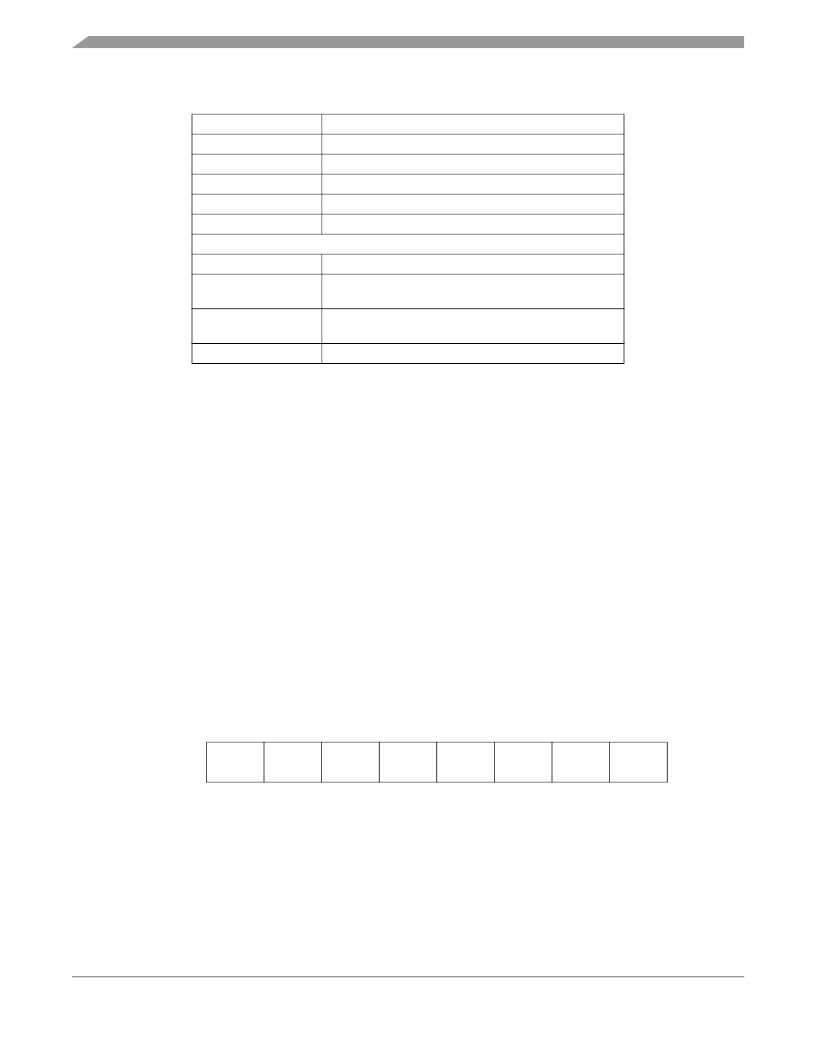
Address: ICGTR5, $FF80 and ICGTR3, $FF81
Bit 7
6
5
4
3
2
1
Bit 0
Read:
TRIM7
TRIM6
TRIM5
TRIM4
TRIM3
TRIM2
TRIM1
TRIM0
Write:
Reset:
Unaffected by reset. Initial value from factory is 1.
Write to this register is by a programming sequence to the Flash memory.
Figure 2-7. ICG User Trim Registers (ICGTR5 and ICGTR3)
相關(guān)PDF資料 |
PDF描述 |
|---|---|
| MC68HC05P9A | HCMOS Microcontroller Unit |
| MC68HC05P9ACDW | HCMOS Microcontroller Unit |
| MC68HC05P9AVDW | HCMOS Microcontroller Unit |
| MC68HC05P9AVP | HCMOS Microcontroller Unit |
| MC68HC05P9ACP | HCMOS Microcontroller Unit |
相關(guān)代理商/技術(shù)參數(shù) |
參數(shù)描述 |
|---|---|
| MC68H705C8A | 制造商:Motorola Inc 功能描述: |
| MC68HC | 制造商:FREESCALE 制造商全稱:Freescale Semiconductor, Inc 功能描述:Power Saving STOP and WAIT Modes |
| MC68HC000 | 制造商:FREESCALE 制造商全稱:Freescale Semiconductor, Inc 功能描述:Microprocessor User Manual Ninth Edition |
| MC68HC000-12/BXAJC | 制造商:Freescale Semiconductor 功能描述: |
| MC68HC000CEI10 | 功能描述:IC MPU 16BIT 10MHZ 68-PLCC RoHS:是 類別:集成電路 (IC) >> 嵌入式 - 微處理器 系列:M680x0 標(biāo)準(zhǔn)包裝:2 系列:MPC8xx 處理器類型:32-位 MPC8xx PowerQUICC 特點(diǎn):- 速度:133MHz 電壓:3.3V 安裝類型:表面貼裝 封裝/外殼:357-BBGA 供應(yīng)商設(shè)備封裝:357-PBGA(25x25) 包裝:托盤 |
發(fā)布緊急采購,3分鐘左右您將得到回復(fù)。