- 您現(xiàn)在的位置:買賣IC網(wǎng) > PDF目錄371038 > MC54F382 (Motorola, Inc.) 4-BIT ARITHMETIC LOGIC UNIT PDF資料下載
參數(shù)資料
| 型號: | MC54F382 |
| 廠商: | Motorola, Inc. |
| 英文描述: | 4-BIT ARITHMETIC LOGIC UNIT |
| 中文描述: | 4位算術邏輯單元 |
| 文件頁數(shù): | 4/6頁 |
| 文件大小: | 162K |
| 代理商: | MC54F382 |

4-186
FAST AND LS TTL DATA
MC54/74F382
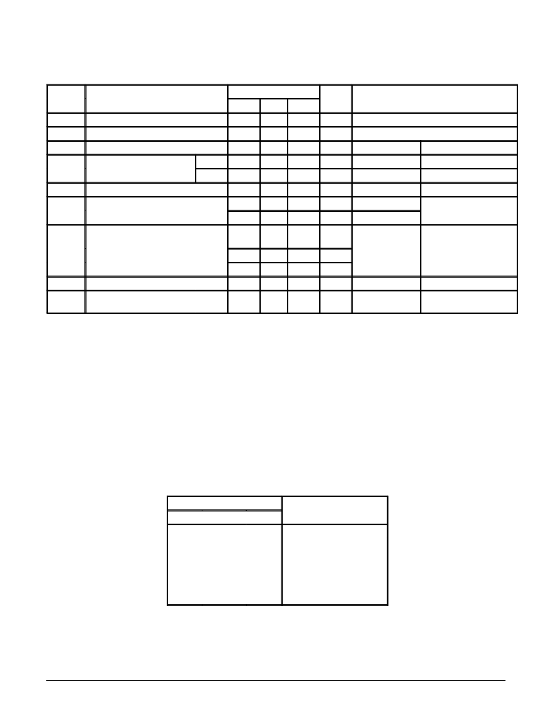
DC CHARACTERISTICS OVER OPERATING TEMPERATURE RANGE
(unless otherwise specified)
Symbol
Parameter
Limits
Unit
Test Conditions
Min
Typ
Max
VIH
VIL
VIK
Input HIGH Voltage
2.0
V
Guaranteed Input HIGH Voltage
Input LOW Voltage
0.8
V
Guaranteed Input LOW Voltage
Input Clamp Diode Voltage
–1.2
V
IIN = –18 mA
IOH = –1.0 mA
IOH = –1.0 mA
IOL = 20 mA
VIN = 2.7 V
VIN = 7.0 V
VCC = MIN
VCC = 4.5 V
VCC = 4.75 V
VCC = MIN
VOH
Output HIGH Voltage
54, 74
2.5
3.4
V
74
2.7
3.4
V
VOL
Output LOW Voltage
0.35
0.5
V
IIH
Input HIGH Current
20
μ
A
VCC = MAX
100
μ
A
IIL
Input LOW Current
S0–S2 Inputs
Other Inputs
–0.6
mA
VIN = 0.5 V
VCC = MAX
–2.4
mA
Cn Input
Output Short Circuit Current (Note 2)
–3.0
mA
IOS
–60
–150
mA
VOUT = 0 V
S0, Cn = HIGH;
Other Inputs GND
VCC = MAX
ICC
Power Supply Current
54
81
mA
VCC = MAX
NOTES:
1. For conditions such as MIN or MAX, use the appropriate value specified under guaranteed operating ranges.
2. Not more than one output should be shorted at a time, nor for more than 1 second.
FUNCTIONAL DESCRIPTION
Signals applied to the Select inputs S0–S2 determine the
mode of operation, as indicated in the Function Select Table.
An extensive listing of input and output levels is shown in the
Truth Table. The circuit performs the arithmetic functions for
either active HIGH or active LOW operands, with output levels
in the same convention. In the Subtract operating modes, it is
necessary to force a carry (HIGH for active HIGH operands,
LOW for active LOW operands) into the Cn input of the least
significant package. Ripple expansion is illustrated in Figure
1. The overflow output OVR is the Exclusive-OR of Cn + 3 and
Cn+4; a HIGH signal on OVR indicates overflow in twos
complement operation. Typical delays for Figure 1 are given
in Figure 2.
FUNCTION SELECT TABLE
Select
Operation
S0
L
H
L
H
L
H
L
H
S1
L
L
H
H
L
L
H
H
S2
L
L
L
L
H
H
H
H
Clear
B Minus A
A Minus B
A Plus B
A
⊕
B
A + B
AB
Preset
H = HIGH Voltage Level L = LOW Voltage Level
相關PDF資料 |
PDF描述 |
|---|---|
| MC74F382 | 4-BIT ARITHMETIC LOGIC UNIT |
| MC74F382DW | 4-BIT ARITHMETIC LOGIC UNIT |
| MC74F382N | Automotive Catalog 220nA Supervisor with 10ms/200ms Selectable Delay Time 5-SOT-23 -40 to 125 |
| MC54HC00AJ | Quad 2-Input NAND Gate |
| MC54HC00 | Quad 2-Input NAND Gate |
相關代理商/技術參數(shù) |
參數(shù)描述 |
|---|---|
| MC54F382J | 制造商:未知廠家 制造商全稱:未知廠家 功能描述:Fixed Point ALU |
| MC54F398J | 制造商:未知廠家 制造商全稱:未知廠家 功能描述:2-Input Digital Multiplexer |
| MC54F399 | 制造商:MOTOROLA 制造商全稱:Motorola, Inc 功能描述:QUAD 2-PORT REGISTER FAST SCHOTTKY TTL |
| MC54F399J | 制造商:未知廠家 制造商全稱:未知廠家 功能描述:2-Input Digital Multiplexer |
| MC54F51J | 制造商:MOTOROLA 制造商全稱:Motorola, Inc 功能描述:DUAL 2-WIDE 2-INPUT, 2-WIDE 3-INPUT AND-OR-INVERT GATE FASTE SCHOTTKY TTL |
發(fā)布緊急采購,3分鐘左右您將得到回復。