- 您現(xiàn)在的位置:買(mǎi)賣(mài)IC網(wǎng) > PDF目錄385567 > MC3479 (ON SEMICONDUCTOR) Stepper Motor Driver(步進(jìn)電機(jī)驅(qū)動(dòng)器) PDF資料下載
參數(shù)資料
| 型號(hào): | MC3479 |
| 廠商: | ON SEMICONDUCTOR |
| 英文描述: | Stepper Motor Driver(步進(jìn)電機(jī)驅(qū)動(dòng)器) |
| 中文描述: | 步進(jìn)電機(jī)驅(qū)動(dòng)器(步進(jìn)電機(jī)驅(qū)動(dòng)器) |
| 文件頁(yè)數(shù): | 5/11頁(yè) |
| 文件大?。?/td> | 182K |
| 代理商: | MC3479 |
MC3479
http://onsemi.com
5
5
Phase A
+ 12 V
MC3479P
CW / CCW
F / HS
OIC
Clk
Bias/Set
56 k
6
7
8
9
10
4
12 13
15
14
3
2
16
V
M
1.0 k
1.0 k
1.0 k
1.0 k
1.0 k
1.0 k
4.0 k
11
L3
L4
L1
L2
0.1 F
+ 12 V
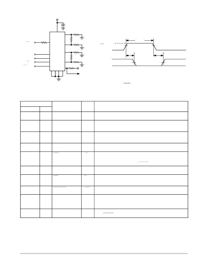
Figure 2. AC Test Circuit
Note: t
r
, t
f
(10% to 90%) for
input signals are
25 ns.
Figure 3. Bias/Set Timing (Refer to Figure 2)
Bias/Set
Input
V
M
PW
BS
V
M
1.0
V
M
1.0
t
PBSD
t
PBSD
(High Impedance)
0
L1 L4
Outputs
PIN FUNCTION DESCRIPTION
Pin No.
Function
Symbol
Description
20
Pin
16
Pin
20
16
Power Supply
V
M
Power supply pin for both the logic circuit and the motor coil current.
Voltage range is + 7.2 to + 16.5 V.
4, 5, 6, 7,
14, 15, 16, 17
4, 5,
12, 13
Ground
GND
Ground pins for the logic circuit and the motor coil current. The physical
configuration of the pins aids in dissipating heat from within the IC
package.
1
1
Clamp Diode Voltage
V
D
This pin is used to protect the outputs where large voltage spikes may
occur as the motor coils are switched. Typically a diode is connected
between this pin and Pin 16. See Figure 12.
2, 3,
18, 19
2, 3,
14, 15
Driver Outputs
L1, L2
L3, L4
High current outputs for the motor coils. L1 and L2 are connected to one
coil, and L3 and L4 to the other coil.
8
6
Bias/Set
B/S
This pin is typically 0.7 volts below V
M
. The current out of this pin (through
a resistor to ground) determines the maximum output sink current. If the pin
is opened (I
BS
< 5.0 A) the outputs assume a high impedance condition,
while the internal logic presets to a Phase A condition.
9
7
Clock
Clk
The positive edge of the clock input switches the outputs to the next
position. This input has no effect if Pin 6 is open.
11
9
Full/Half Step
F/HS
When low (Logic “0”), each clock input pulse will cause the motor to rotate
one full step. When high, each clock pulse will cause the motor to rotate
one
half step. See Figure 7 for sequence.
12
10
Clockwise/
Counterclockwise
CW/
CCW
This input allows reversing the rotation of the motor. See Figure 7 for
sequence.
10
8
Output Impedance
Control
OIC
This input is relevant only in the half step mode (Pin 9 > 2.0 V). When low
(Logic “0”), the two driver outputs of the non
energized coil will be in a high
impedance condition. When high the same driver outputs will be at a low
impedance referenced to V
M
. See Figure 7.
13
11
Phase A
Ph A
This open
collector output indicates (when low) that the driver outputs are
in the Phase A condition (L1 = L3 = V
OHD
, L2 = L4 = V
OLD
).
相關(guān)PDF資料 |
PDF描述 |
|---|---|
| MC44BC375 | PLL Tuned VHF Audio/ Video High Integration Modulator ICs |
| MC44BC375J | PLL Tuned VHF Audio/ Video High Integration Modulator ICs |
| MC44BC375JD | PLL Tuned VHF Audio/ Video High Integration Modulator ICs |
| MC44BC375T | PLL Tuned VHF Audio/ Video High Integration Modulator ICs |
| MC44BC375TD | PLL Tuned VHF Audio/ Video High Integration Modulator ICs |
相關(guān)代理商/技術(shù)參數(shù) |
參數(shù)描述 |
|---|---|
| MC34791 | 制造商:SPC Multicomp 功能描述:CONNECTOR FPC 1.25MM 6WAY 制造商:SPC Multicomp 功能描述:CONNECTOR, FPC, 1.25MM, 6WAY |
| MC34793 | 制造商:SPC Multicomp 功能描述:CONNECTOR FPC 1.25MM 8WAY 制造商:SPC Multicomp 功能描述:CONNECTOR, FPC, 1.25MM, 8WAY |
| MC34795 | 制造商:SPC Multicomp 功能描述:CONNECTOR FPC 1.25MM 8WAY 制造商:SPC Multicomp 功能描述:CONNECTOR, FPC, 1.25MM, 8WAY |
| MC34797 | 制造商:SPC Multicomp 功能描述:CONNECTOR FPC 1.25MM 10WAY |
| MC34799 | 制造商:SPC Multicomp 功能描述:CONNECTOR FPC 1.25MM 10WAY 制造商:SPC Multicomp 功能描述:CONNECTOR, FPC, 1.25MM, 10WAY |
發(fā)布緊急采購(gòu),3分鐘左右您將得到回復(fù)。