- 您現(xiàn)在的位置:買賣IC網(wǎng) > PDF目錄1948 > MC33742EPR2 (Freescale Semiconductor)IC SYSTEM BASE W/CAN 48-QFN PDF資料下載
參數(shù)資料
| 型號: | MC33742EPR2 |
| 廠商: | Freescale Semiconductor |
| 文件頁數(shù): | 50/71頁 |
| 文件大小: | 0K |
| 描述: | IC SYSTEM BASE W/CAN 48-QFN |
| 標(biāo)準包裝: | 2,000 |
| 應(yīng)用: | 自動 |
| 接口: | SPI |
| 電源電壓: | 5.5 V ~ 18 V |
| 封裝/外殼: | 48-VFQFN 裸露焊盤 |
| 供應(yīng)商設(shè)備封裝: | 48-QFN-EP(7x7) |
| 包裝: | 帶卷 (TR) |
| 安裝類型: | 表面貼裝 |
第1頁第2頁第3頁第4頁第5頁第6頁第7頁第8頁第9頁第10頁第11頁第12頁第13頁第14頁第15頁第16頁第17頁第18頁第19頁第20頁第21頁第22頁第23頁第24頁第25頁第26頁第27頁第28頁第29頁第30頁第31頁第32頁第33頁第34頁第35頁第36頁第37頁第38頁第39頁第40頁第41頁第42頁第43頁第44頁第45頁第46頁第47頁第48頁第49頁當(dāng)前第50頁第51頁第52頁第53頁第54頁第55頁第56頁第57頁第58頁第59頁第60頁第61頁第62頁第63頁第64頁第65頁第66頁第67頁第68頁第69頁第70頁第71頁
Analog Integrated Circuit Device Data
54
Freescale Semiconductor
33742
FUNCTIONAL DEVICE OPERATION
LOGIC COMMANDS AND REGISTERS
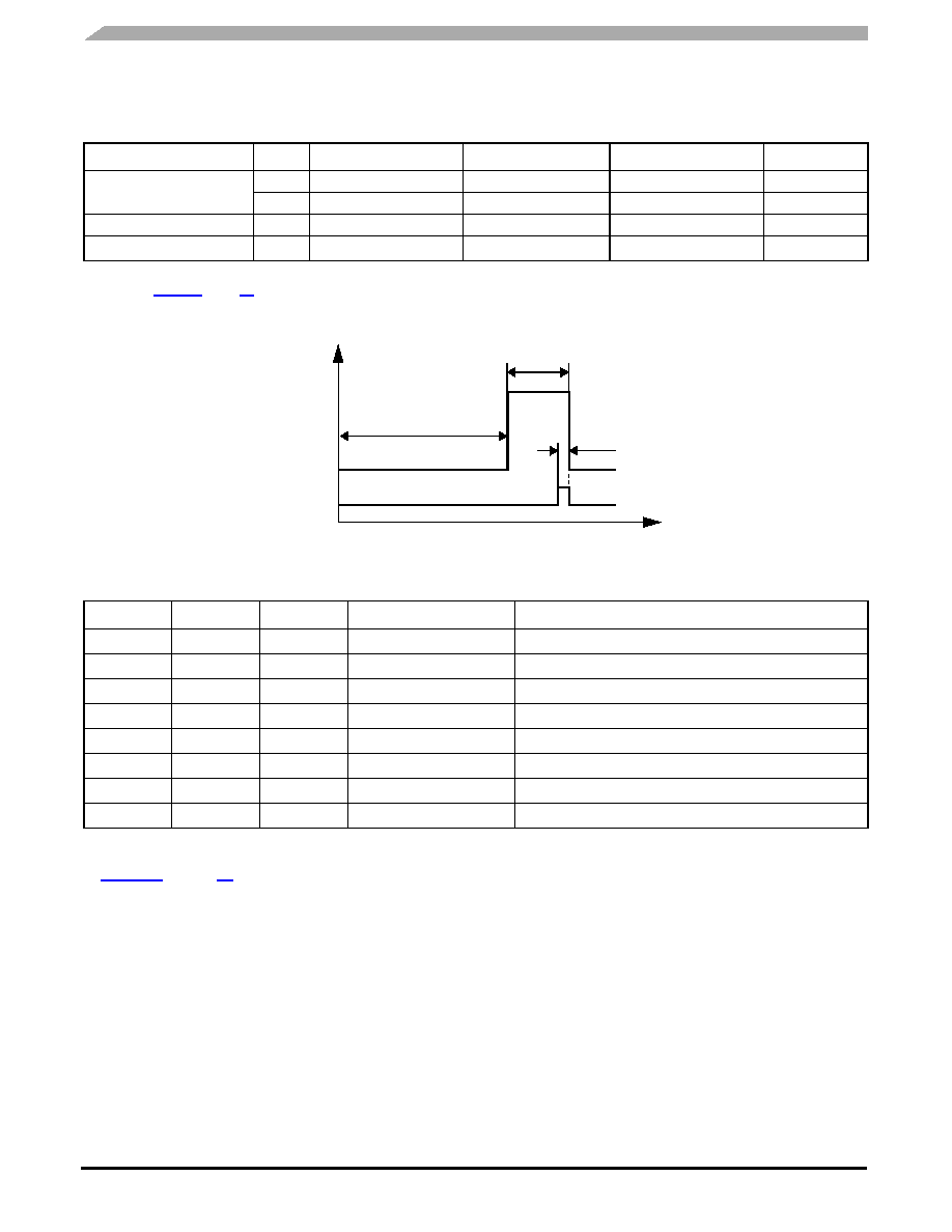
Figure 30. HS Operation When Cyclic Sense Is Selected
LOW POWER CONTROL REGISTER (LPC)
The state of HS in Stop and Sleep modes (HS permanently OFF or HS cyclic).
Enable or disable of the forced wake-up function (SBC automatic wake-up after time spent in Sleep or Stop modes; time is
defined by the TIM2 sub register).
Enable or disable the sense of the wake-up inputs (Lx) at the sampling point of the Cyclic Sense period (LX2HS bit). (Refer to
Reset Control Register (RCR) on page 49 for details of the LPC register setup required for proper cyclic sense or direct wake-
up operation.
The LPC register also reports the CANH and RXD diagnostic.
Table 34. TIM2 Timing and CANL Failure Diagnostic Register
TIM2
R/W
D3
D2
D1
D0
$101b
W
1
CSP2
CSP1
CSP0
R
CANL2VDD
CANL2BAT
CANL2GND
TXPD
Reset Value
–
0
Reset Condition (Write)(64)
–
POR, RESET
Notes
64.
See Table 13, page 46, for definitions of reset conditions.
Table 35. TIM2 Control Bits
CSP2
CSP1
CSP0
Cyclic Sense Timing (ms)
Parameter
0
4.6
Cyclic Sense/FWU Timing 1
0
1
9.25
Cyclic Sense/FWU Timing 2
0
1
0
18.5
Cyclic Sense/FWU Timing 3
0
1
37
Cyclic Sense/FWU Timing 4
1
0
74
Cyclic Sense/FWU Timing 5
1
0
1
95.5
Cyclic Sense/FWU Timing 6
1
0
191
Cyclic Sense/FWU Timing 7
1
388
Cyclic Sense/FWU Timing 8
Cyclic Sense Timing, OFF Time
time
HS
Sample
10
s
HS OFF
HS ON
Lx Sampling Point
Cyclic Sense Timing,
ON Time
發(fā)布緊急采購,3分鐘左右您將得到回復(fù)。