- 您現(xiàn)在的位置:買(mǎi)賣(mài)IC網(wǎng) > PDF目錄11718 > MC33560DTB (ON Semiconductor)OC PWR MGMT READERS/CPLR 24TSSOP PDF資料下載
參數(shù)資料
| 型號(hào): | MC33560DTB |
| 廠商: | ON Semiconductor |
| 文件頁(yè)數(shù): | 20/26頁(yè) |
| 文件大?。?/td> | 0K |
| 描述: | OC PWR MGMT READERS/CPLR 24TSSOP |
| 標(biāo)準(zhǔn)包裝: | 62 |
| 系列: | * |
| 應(yīng)用: | * |
| 接口: | * |
| 電源電壓: | * |
| 封裝/外殼: | 24-TSSOP(0.220",5.60mm 寬) |
| 供應(yīng)商設(shè)備封裝: | 24-TSSOP |
| 包裝: | 管件 |
| 安裝類(lèi)型: | 表面貼裝 |
第1頁(yè)第2頁(yè)第3頁(yè)第4頁(yè)第5頁(yè)第6頁(yè)第7頁(yè)第8頁(yè)第9頁(yè)第10頁(yè)第11頁(yè)第12頁(yè)第13頁(yè)第14頁(yè)第15頁(yè)第16頁(yè)第17頁(yè)第18頁(yè)第19頁(yè)當(dāng)前第20頁(yè)第21頁(yè)第22頁(yè)第23頁(yè)第24頁(yè)第25頁(yè)第26頁(yè)
MC33560
http://onsemi.com
3
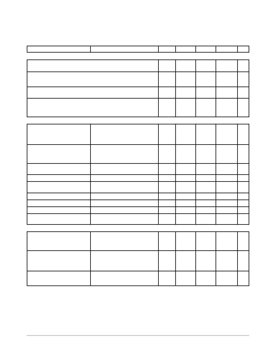
ELECTRICAL CHARACTERISTICS These specifications are written in the same style as common for standard
integrated circuits. The convention considers current flowing into the pin (sink current) as positive and current flowing out of the pin
(source current) as negative. (Conditions: VBAT = 4.0 V, VCC = 5.0 V nom, PWRON = VBAT , Operating Mode, ICC = 10 mA, 25°C ≤ TA
≤ 85°C, L1 = 47 mH, RLIM = 0 W, CRDVCC capacitor = 10 mF, unless otherwise noted.)
Characteristic
Test Conditions
Symbol
Min
Typ
Max
Unit
BATTERY POWER SUPPLY SECTION
Supply Voltage Range
Normal operating range extended operating range (Note 4)
VBAT
2.2
1.8
6.0
6.6
V
MC33560 Standby Quiescent Current
PWRON = GND, CRDCON = GND, ASYCLKIN = GND, VBAT = 6.0 V,
All Other Logic Inputs and Outputs Open
IoBAT
30
mA
DC Operating Current
ICC = 10 mA; VCC = 5.0 V, VBAT = 6.0 V
IBATop
12.5
mA
VBAT Undervoltage Detection:
Upper Threshold
Lower Threshold
Hysteresis
1.6
1.4
0.2
V
VCC = 5.0 V NOMINAL POWER SUPPLY SECTION
Output Voltage
2.2 V
v VBAT v 6.0 V
1.0 mA
v ICC v 25 mA
3.0 V
v VBAT v 6.0 V
1.0 mA
v ICC v 60 mA
VCC
4.75
4.60
5.0
5.25
5.40
V
Card VCC Undervoltage Detection:
Upper Threshold
Lower Threshold
Switching Hysteresis
(RDYMOD Output)
(See Table 4)
VT5H
VT5L
VHYS5
4.2
120
4.5
180
VCC 0.14
V
mV
Peak Output Current
VCC = 4.0 V, Internally Limited
(RDYMOD = L)
ICClim
80
mA
Current limit timeout
VCC = 4.0 V
td
160
ms
Startup Current
VCC = 2.0 V; 0°C to +85°C
40
°C to 0°C
ICCst
80
50
mA
Low Side Switch Saturation Voltage
IL = 50 mA, Pin 22
Vsat22
100
160
mV
Rectifier on Saturation Voltage
IL = 50 mA, Pin 22 to Pin 13
VFsat22
400
520
mV
Converter Switching Frequency
TA = 25°C
fsw
120
kHz
Shutdown Current
(Card access deactivated)
PWRON = GND, VCC = 2.0 V
ISD
80
mA
VCC = 3.0 V NOMINAL POWER SUPPLY SECTION (VBAT = 2.5 V, ICC = 5.0 mA)
Output Voltage
2.2 V
v VBAT v 6.0 V
1.0 mA
v ICC v 10 mA
2.5 V
v VBAT v 6.0 V
1.0 mA
v ICC v 50 mA
VCC
2.75
2.60
3.0
3.25
3.40
V
Card VCC Undervoltage Detection:
Upper Threshold
Lower Threshold
Switching Hysteresis
(RDYMOD Output)
(See Table 4)
VT3H
VT3L
VHYS3
2.4
80
2.7
110
VCC 0.1
V
mV
Startup Current
Shutdown Current
(Card access deactivated)
VCC = 2.0 V
PWRON = GND, VCC = 2.0 V
ICCst
ISD
50
mA
6. Pin loading = 30 pF, except INVOUT = 15 pF.
7. As the clock buffer is optimized for low power consumption and hence not symmetrical, clock signal duty cycle is guaranteed for divide
by 2 and divide by 4 ratio.
8. In either direction.
相關(guān)PDF資料 |
PDF描述 |
|---|---|
| MC100E446FNR2 | IC CONV 4BIT SER/PAR ECL 28-PLCC |
| D38999/26WG41SN | CONN PLUG 41POS STRAIGHT W/SCKT |
| D38999/24JD18HN | CONN RCPT 18POS JAM NUT W/PINS |
| MCZ33797EK | IC SQUIB DRIVER 4-CH 32-SOIC |
| MCZ33889BEG | IC SYSTEM BASIS W/CAN 28-SOIC |
相關(guān)代理商/技術(shù)參數(shù) |
參數(shù)描述 |
|---|---|
| MC33560DTBR2 | 功能描述:輸入/輸出控制器接口集成電路 3V/5V Smartcard RoHS:否 制造商:Silicon Labs 產(chǎn)品: 輸入/輸出端數(shù)量: 工作電源電壓: 最大工作溫度:+ 85 C 最小工作溫度:- 40 C 安裝風(fēng)格:SMD/SMT 封裝 / 箱體:QFN-64 封裝:Tray |
| MC33560DTBR2G | 功能描述:輸入/輸出控制器接口集成電路 3V/5V Smartcard Power Management RoHS:否 制造商:Silicon Labs 產(chǎn)品: 輸入/輸出端數(shù)量: 工作電源電壓: 最大工作溫度:+ 85 C 最小工作溫度:- 40 C 安裝風(fēng)格:SMD/SMT 封裝 / 箱體:QFN-64 封裝:Tray |
| MC33560DW | 功能描述:輸入/輸出控制器接口集成電路 3V/5V Smartcard RoHS:否 制造商:Silicon Labs 產(chǎn)品: 輸入/輸出端數(shù)量: 工作電源電壓: 最大工作溫度:+ 85 C 最小工作溫度:- 40 C 安裝風(fēng)格:SMD/SMT 封裝 / 箱體:QFN-64 封裝:Tray |
| MC33560DWR2 | 功能描述:輸入/輸出控制器接口集成電路 3V/5V Smartcard RoHS:否 制造商:Silicon Labs 產(chǎn)品: 輸入/輸出端數(shù)量: 工作電源電壓: 最大工作溫度:+ 85 C 最小工作溫度:- 40 C 安裝風(fēng)格:SMD/SMT 封裝 / 箱體:QFN-64 封裝:Tray |
| MC33560DWR2G | 功能描述:輸入/輸出控制器接口集成電路 3V/5V Smartcard Power Management RoHS:否 制造商:Silicon Labs 產(chǎn)品: 輸入/輸出端數(shù)量: 工作電源電壓: 最大工作溫度:+ 85 C 最小工作溫度:- 40 C 安裝風(fēng)格:SMD/SMT 封裝 / 箱體:QFN-64 封裝:Tray |
發(fā)布緊急采購(gòu),3分鐘左右您將得到回復(fù)。