- 您現(xiàn)在的位置:買(mǎi)賣(mài)IC網(wǎng) > PDF目錄371019 > MC14C89 (Motorola, Inc.) QUAD LOW POWER LINE RECEIVERS PDF資料下載
參數(shù)資料
| 型號(hào): | MC14C89 |
| 廠商: | Motorola, Inc. |
| 英文描述: | QUAD LOW POWER LINE RECEIVERS |
| 中文描述: | 四低功率線路接收機(jī) |
| 文件頁(yè)數(shù): | 2/6頁(yè) |
| 文件大?。?/td> | 118K |
| 代理商: | MC14C89 |

MC14C89B, AB
2
MOTOROLA ANALOG IC DEVICE DATA
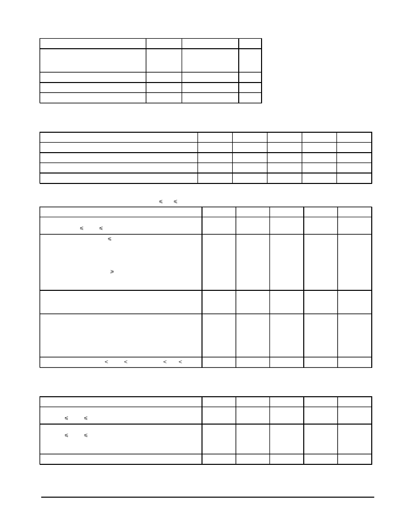
MAXIMUM RATINGS
Rating
Symbol
Value
Unit
Power Supply Voltage
VCC(max)
VCC(min)
VCC
+ 7.0
– 0.5
Vdc
Input Voltage
Vin
IO
TJ
±
30
Vdc
Output Load Current
Self–Limiting
–
Junction Temperature
–65, +150
°
C
Devices should not be operated at these limits. The “Recommended Operating Conditions” table provides
for actual device operation.
RECOMMENDED OPERATING CONDITIONS
Characteristic
Symbol
Min
Typ
Max
Unit
Power Supply Voltage
VCC
Vin
IO
TA
4.5
5.0
5.5
Vdc
Input Voltage
–25
–
25
Vdc
Output Current Capability
–7.5
–
6.0
mA
Operating Ambient Temperature
–40
–
85
°
C
All limits are not necessarily functional concurrently.
ELECTRICAL CHARACTERISTICS
(–40
°
C
TA
+85
°
C, unless otherwise noted.)*
Characteristic
Symbol
Min
Typ
Max
Unit
Supply Current (Iout = 0)
ICC @ +4.5 V
VCC
+5.5 V
ICC
–
330
700
μ
A
Output Voltage – High, Vin
Iout = –20
μ
A
0.4 V (See Figures 2 and 3)
VCC = 4.5 V
VCC = 5.5 V
VCC = 4.5 V
VCC = 5.5 V
2.4 V
VCC = 4.5 V
VCC = 5.5 V
Iout = –3.2 mA
Output Voltage – Low, Vin
Iout = 3.2 mA
VOH
VOL
3.5
3.5
2.5
2.5
–
–
3.8
4.8
3.7
4.7
0.1
0.1
–
–
–
–
0.4
0.4
Vdc
Output Short Circuit Current** (VCC = 5.5 V, see Figure 4)
Normally High Output shorted to ground
Normally Low Output shorted to VCC
IOS
–35
–
–13.9
+10.3
–
35
mA
Input Threshold Voltage (VCC = 5.0 V)
(MC14C89AB, see Figure 5)
Low Level
High Level
(MC14C89B, see Figure 6)
Low Level
High Level
VIL
VIH
VIL
VIH
0.75
1.6
0.75
1.0
0.95
1.90
0.95
1.3
1.25
2.25
1.25
1.5
Vdc
Input Impedance (+4.5 V
VCC
+5.5 V –25 V
Vin
+25 V)
3.0
5.5
7.0
k
*
* Typicals reflect performance @ TA = 25
°
C
**Only one output shorted at a time, for not more than 1.0 seconds.
TIMING CHARACTERISTICS
(TA = +25
°
C, unless otherwise noted.)
Characteristic
Symbol
Min
Typ
Max
Unit
Output Transition Time (10% to 90%)
4.5 V
VCC
5.5 V
tT
–
0.08
0.30
μ
s
Propagation Delay Time
4.5 V
VCC
Output Low–to–High
Output High–to–Low
5.5 V
tPLH
tPHL
–
–
3.35
2.55
6.0
6.0
μ
s
Input Noise Rejection (see Figure 9)
1.0
1.5
–
μ
s
相關(guān)PDF資料 |
PDF描述 |
|---|---|
| MC14C89ABD | QUAD LOW POWER LINE RECEIVERS |
| MC14C89ABP | OC-48,24,12 SONET SDH Multi-rate Transceiver 100-HTQFP -40 to 85 |
| MC14C89BP | OC-48,24,12 SONET SDH Multi-rate Transceiver 100-HTQFP -40 to 85 |
| MC14LC5447 | Calling Line Identification(CLID) Receiver With Ring Detector(帶振鈴檢測(cè)器的撥號(hào)線識(shí)別接收器) |
| MC14LC5481 | PCM Codec-Filter(PCM 編解碼-濾波器) |
相關(guān)代理商/技術(shù)參數(shù) |
參數(shù)描述 |
|---|---|
| MC14C89AB | 制造商:Motorola Inc 功能描述: |
| MC14E-10-6PN-A105 | 制造商:ITT Interconnect Solutions 功能描述:MC14E-10-6PN-A105 - Bulk |
| MC14E-10-6SN | 制造商:ITT Interconnect Solutions 功能描述:021405-0000 - Bulk |
| MC14E-10-6SN-A105 | 制造商:ITT Interconnect Solutions 功能描述:MC14E-10-6SN-A105 - Bulk |
| MC14E-10-6SW | 制造商:ITT Interconnect Solutions 功能描述:MC14E-10-6SW - Bulk |
發(fā)布緊急采購(gòu),3分鐘左右您將得到回復(fù)。