- 您現(xiàn)在的位置:買賣IC網(wǎng) > PDF目錄385566 > MC14598B (ON SEMICONDUCTOR) 8 Bit Bus Compatible Latches(八位總線型鎖存器) PDF資料下載
參數(shù)資料
| 型號: | MC14598B |
| 廠商: | ON SEMICONDUCTOR |
| 英文描述: | 8 Bit Bus Compatible Latches(八位總線型鎖存器) |
| 中文描述: | 8位總線兼容閥門(八位總線型鎖存器) |
| 文件頁數(shù): | 1/7頁 |
| 文件大?。?/td> | 136K |
| 代理商: | MC14598B |
Semiconductor Components Industries, LLC, 2006
March, 2006
Rev. 5
1
Publication Order Number:
MC14598B/D
MC14598B
8Bit BusCompatible
Latches
The MC14598B is an 8
bit latch addressed with an external binary
address. The 8 latch
outputs are high drive, three
state and bus line
compatible. The drive capability allows direct applications with MPU
systems such as the Motorola 6800 family.
The latches of the MC14598B are accessed via the Address pins,
A0, A1, and A2.
All 8 outputs from the latches are available in parallel when Enable
is in the low state. Data is entered into a selected latch from the Data
pin when the Strobe is high. Master reset is available on both parts.
Serial Data Input
Three
State Bus Compatible Parallel Outputs
Three
State Control Pin (Enable) TTL Compatible Input
Open Drain Full Flag (Multiple Latch Wire
O Ring)
Master Reset
Level Shifting Inputs on All Except Enable
Diode Protection — All Inputs
Supply Voltage Range — 3.0 Vdc to 18 Vdc
Capable of Driving TTL Over Rated Temperature Range
With Fanout as Follows:
1 TTL Load
4 LSTTL Loads
This device is available in Pb
free package(s). Specifications herein
apply to both standard and Pb
free devices. Please see our website at
www.onsemi.com for specific Pb
free orderable part numbers, or
contact your local ON Semiconductor sales office or representative.
MAXIMUM RATINGS
(Voltages Referenced to V
SS
) (Note 1.)
Symbol
Parameter
Value
Unit
V
DD
DC Supply Voltage Range
0.5 to +18.0
V
V
in
Input Voltage Range,
Enable (DC or Transient)
0.5 to V
DD
+ 0.5
V
V
in
Input Voltage Range, All Other
Inputs (DC or Transient)
0.5 to V
DD
+ 12
V
V
out
Output Voltage Range,
(DC or Transient)
0.5 to V
DD
+ 0.5
V
I
in
, I
out
Input or Output Current
(DC or Transient) per Pin
±
10
mA
P
D
Power Dissipation,
per Package (Note 2.)
500
mW
T
A
Ambient Temperature Range
55 to +125
°
C
T
stg
Storage Temperature Range
65 to +150
°
C
T
L
Lead Temperature
(8
Second Soldering)
260
°
C
1. Maximum Ratings are those values beyond which damage to the device
may occur.
2. Temperature Derating:
Plastic “P and D/DW” Packages: – 7.0 mW/ C From 65 C To 125 C
http://onsemi.com
A
WL, L
YY, Y
WW, W
= Assembly Location
= Wafer Lot
= Year
= Work Week
Device
Package
Shipping
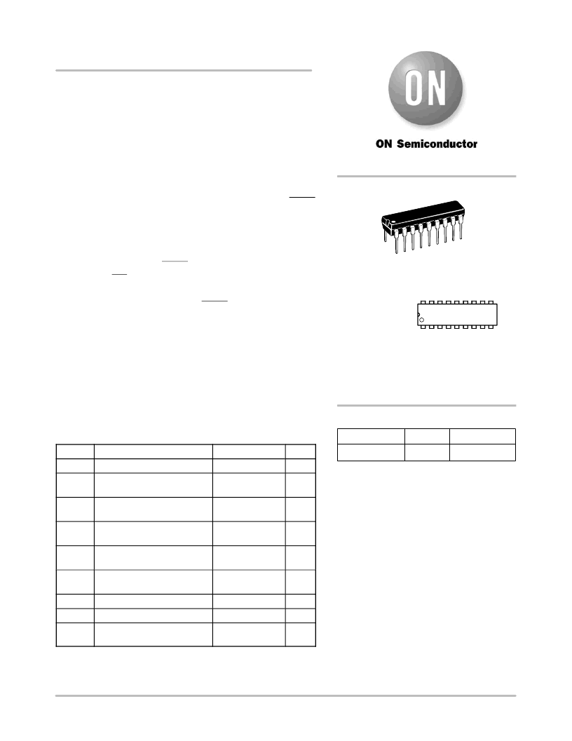
ORDERING INFORMATION
MC14598BCP
PDIP
18
20/Rail
MARKING
DIAGRAMS
1
18
PDIP
18
P SUFFIX
CASE 707
MC14598BCP
AWLYYWW
This device contains protection circuitry to guard
against damage due to high static voltages or electric
fields. However, precautions must be taken to avoid ap-
plications of any voltage higher than maximum rated
voltages to this high
impedance circuit. For proper
operation, V
in
and V
out
should be constrained to the
range V
SS
(V
in
or V
out
)
Unused inputs must always be tied to an appropriate
logic voltage level (e.g., either V
SS
or V
DD
). Unused out-
puts must be left open.
V
DD
.
相關(guān)PDF資料 |
PDF描述 |
|---|---|
| MC1471 | Internally Compensated, High Performance Operational Amplifier |
| MC1489A | Quad Line EIA-232D Receivers(RS-232四線接收器) |
| MC1H3 | High Voltage Power Module Users Guide |
| MC33023DWG | High Speed Single−Ended PWM Controller |
| MC33023DWR2 | High Speed Single−Ended PWM Controller |
相關(guān)代理商/技術(shù)參數(shù) |
參數(shù)描述 |
|---|---|
| MC14598BCP | 功能描述:閉鎖 3-18V 9-Bit RoHS:否 制造商:Micrel 電路數(shù)量:1 邏輯類型:CMOS 邏輯系列:TTL 極性:Non-Inverting 輸出線路數(shù)量:9 高電平輸出電流: 低電平輸出電流: 傳播延遲時(shí)間: 電源電壓-最大:12 V 電源電壓-最小:5 V 最大工作溫度:+ 85 C 最小工作溫度:- 40 C 封裝 / 箱體:SOIC-16 封裝:Reel |
| MC14598BCPG | 功能描述:閉鎖 3-18V 9-Bit Bus-Compatible RoHS:否 制造商:Micrel 電路數(shù)量:1 邏輯類型:CMOS 邏輯系列:TTL 極性:Non-Inverting 輸出線路數(shù)量:9 高電平輸出電流: 低電平輸出電流: 傳播延遲時(shí)間: 電源電壓-最大:12 V 電源電壓-最小:5 V 最大工作溫度:+ 85 C 最小工作溫度:- 40 C 封裝 / 箱體:SOIC-16 封裝:Reel |
| MC1459BFR1 | 制造商:Rochester Electronics LLC 功能描述:- Bulk |
| MC-146 | 制造商:EPSONTOYOCOM 制造商全稱:Epson ToYoCom 功能描述:LOW PROFILE SMD |
| MC-146 32.768000KHz12.5 }20 | 制造商:Epson Toyocom Corporation 功能描述:Cut Tape |
發(fā)布緊急采購,3分鐘左右您將得到回復(fù)。