- 您現(xiàn)在的位置:買賣IC網 > PDF目錄369899 > MC145442B (Motorola, Inc.) Single-Chip 300-Baud Modem PDF資料下載
參數(shù)資料
| 型號: | MC145442B |
| 廠商: | Motorola, Inc. |
| 英文描述: | Single-Chip 300-Baud Modem |
| 中文描述: | 單芯片300波特調制解調器 |
| 文件頁數(shù): | 4/12頁 |
| 文件大小: | 111K |
| 代理商: | MC145442B |

MC145442B
MC145443B
4
MOTOROLA
TEST
INPUT
600
600
VDD
RTLA
20
17
15
16
TEST
OUTPUT
4
CDT
RxA1
CCDT
CFB
0.1
μ
F
10
FB
RxD
5
11
Dout
Din
TxD
Xin
9
8
Xout
TLA
TxA
RxA2
MC145442B
MC145443B
0.1
μ
F
3.579 MHz
±
0.1%
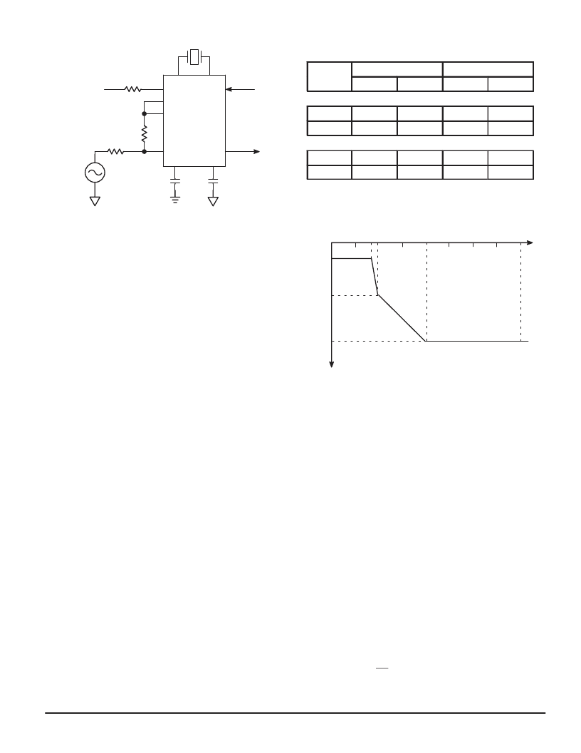
Figure 1. AC Characteristics Evaluation Circuit
PIN DESCRIPTIONS
VDD
Positive Power Supply (Pin 6)
This pin is normally tied to 5.0 V.
VSS
Negative Power Supply (Pin 12)
This pin is normally tied to 0 V.
VAG
Analog Ground (Pin 19)
Analog ground is internally biased to (VDD – VSS)/2. This
pin must be decoupled by a capacitor from VAG to VSS and a
capacitor from VAG to VDD. Analog ground is the common
bias line used in the switched capacitor filters, limiter, and
slicer in the demodulation circuitry.
TLA
Transmit Level Adjust (Pin 20)
This pin is used to adjust the transmit level. Transmit level
adjustment range is typically from –12 dBm to –9 dBm. (See
Applications Information.
)
TxD
Transmit Data (Pin 11)
Binary information is input to the transmit data pin. Data
entered for transmission is modulated using FSK techniques.
A logic high input level represents a mark and a logic low
represents a space (see Table 1).
TxA
Transmit Carrier (Pin 17)
This is the output of the line driver amplifier. The transmit
carrier is the digitally synthesized sine wave output of the
modulator derived from a crystal oscillator reference. When a
3.579 MHz crystal is used the frequency outputs shown in
Table 1 apply. (See
Applications Information
.)
Table 1. Bell 103 and CCITT V.21
Frequency Characteristics
Originate Mode
Answer Mode
Data
Transmit
Receive
Transmit
Receive
Bell 103 (MC145443B)
Space
1070 Hz
2025 Hz
2025 Hz
1070 Hz
Mark
1270 Hz
2225 Hz
2225 Hz
1270 Hz
CCITT V.21 (MC145442B)
Space
1180 Hz
1850 Hz
1850 Hz
1180 Hz
Mark
980 Hz
1650 Hz
1650 Hz
980 Hz
NOTE: Actual frequencies may be
±
5 Hz assuming 3.579545 MHz
crystal is used.
15 dB/OCTAVE
256
64
16
3.4 4
2
0
0
–20
–25
–55
–60
T
MAXIMUMLEVEL OF OUT–OF–BAND ENERGY
RELATIVE TO THE TRANSMIT CARRIER LEVEL INTO 600
(kHz)
Figure 2. Out–of–Band Energy
ExI
External Input (Pin 18)
The external input is the non–inverting input to the line
driver. It is provided to combine an auxiliary audio signal or
speech signal to the phone line using the line driver. This pin
should be connected to VAG if not used. The average level
must be the same as VAG to maintain proper operation. (See
Applications Information
.)
DSI
Driver Summing Input (Pin 1)
The driver summing input may be used to connect an ex-
ternal signal, such as a DTMF dialer, to the phone line. A
series resistor, RDSI, is needed to define the voltage gain
AV (see
Applications Information
and Figure 6). When ap-
plying a signal to the DSI pin, the modulator should be
squelched by bringing SQT (pin 14) to a logic high level. The
voltage gain, AV, is calculated by the formula AV = –Rf/RDSI
(where Rf
≈
20 k
). For example, a 20 k
resistor for RDSI
will provide unity gain (AV = –20 k
/20 k
= –1). This pin
must
be left open f not used.
RxD
Receive Data (Pin 6)
The receive data output pin presents the digital binary data
resulting from the demodulation of the receive carrier. If no
carrier is present, CD high, the receive data output (RxD) is
clamped high.
相關PDF資料 |
PDF描述 |
|---|---|
| MC145443B | Single-Chip 300-Baud Modem |
| MC145442BP | Single-Chip 300-Baud Modem |
| MC145443BDW | Single-Chip 300-Baud Modem |
| MC145443BP | Single-Chip 300-Baud Modem |
| MC145442DW | Single-Chip 300-Baud Modem |
相關代理商/技術參數(shù) |
參數(shù)描述 |
|---|---|
| MC145443P | 制造商:Motorola Inc 功能描述: |
| MC145446AFW | 制造商:Rochester Electronics LLC 功能描述:- Bulk 制造商:Motorola Inc 功能描述: 制造商:MOTOROLA 功能描述: |
| MC145447DW | 制造商:Motorola Inc 功能描述:CALLER NUMBER ID CIRCUIT, 16 Pin, Plastic, SOP |
| MC145447DWR2 | 制造商:Motorola Inc 功能描述:TELEPHONE MULTIFUNCTION CKT, 16 Pin Plastic SOP |
| MC145447P | 制造商:Motorola Inc 功能描述: |
發(fā)布緊急采購,3分鐘左右您將得到回復。