- 您現(xiàn)在的位置:買賣IC網(wǎng) > PDF目錄369899 > MC145442 (Motorola, Inc.) Single-Chip 300-Baud Modem PDF資料下載
參數(shù)資料
| 型號: | MC145442 |
| 廠商: | Motorola, Inc. |
| 英文描述: | Single-Chip 300-Baud Modem |
| 中文描述: | 單芯片300波特調(diào)制解調(diào)器 |
| 文件頁數(shù): | 5/12頁 |
| 文件大?。?/td> | 224K |
| 代理商: | MC145442 |

MC145442
MC145443
MOTOROLA
5
RxA2, RxA1
Receive Carrier (Pins 15, 16)
The receive carrier is the FSK input to the demodulator
through the receive band–pass filter. RxA1 is the non–invert-
ing input and RxA2 is the inverting input of the receive hybrid
(duplexer) operational amplifier.
LB
Analog Loopback (Pin 2)
When a high level is applied to this pin (SQT must be low),
the analog loopback test is enabled. The analog loopback
test connects the TxA pin to the RxA2 pin and the RxA1 to
analog ground. In loopback, the demodulator frequencies
are switched to the modulation frequencies for the selected
mode. (See Tables 1 and 2 and Figures 4c and 4d.)
When LB is connected to analog ground (VAG), the modu-
lator generates an echo cancellation tone of 2100 Hz for
MC145442 CCITT V.21 and 2225 Hz for MC145443 Bell 103
systems. For normal operation, this pin should be at a logic
low level (VSS).
The power–down mode is enabled when both LB and SQT
are connected to a logic high level (see Table 2).
Table 2. Functional Table
MODE
Pin 13
SQT
Pin 14
LB
Pin 2
Operating Mode
1
0
0
Originate Mode
0
0
0
Answer Mode
X
0
VAG (VDD/2)
1
Echo Tone
X
0
Analog Loopback
X
1
0
Squelch Mode
X
1
VAG (VDD/2)
1
Squelch Mode
X
1
Power Down
MODE
Mode (Pin 13)
This input selects the pair of transmit and frequencies
used during modulation and demodulation. When a logic
high level is placed on this input, originate (Bell) or channel 1
(CCITT) is selected. When a low level is placed on this input,
answer (Bell) or channel 2 (CCITT) is selected. (See
Tables 1 and 2 and Figure 4.)
CDT
Carrier Detect Timing (Pin 4)
A capacitor on this pin to VSS sets the amount of time the
carrier must be present before CD goes low (see
Applica-
tions Information
for the capacitor values).
CD
Carrier Detect Output (Pin 3)
This output is used to indicate when a carrier has been
sensed by the carrier detect circuit. This output goes to a
logic low level when a valid signal above the maximum
threshold level (defined by CDA, Pin 7) is maintained on the
input to the hybrid circuit longer then the response (defined
by CDT, Pin 4). This pin is held at the logic low level until the
signal falls below the maximum threshold level for longer
than the turn off time. (See
Applications Information
and
Figure 5.)
CDA
Carrier Detect Adjust (Pin 7)
An external voltage may be applied to this pin to adjust the
carrier detect threshold. The threshold hysteresis is internally
fixed at 3 dB (see
Applications Information
).
Xout, Xin
Crystal Oscillator (Pins 8, 9)
A crystal reference oscillator is formed when a 3.579 MHz
crystal is connected between these two pins. Xout (Pin 8) is
the output of the oscillator circuit, and Xin (Pin 9) is the input
to the oscillator circuit. When using an external clock, apply
the clock to the Xin (Pin 9) pin and leave Xout (Pin 8) open. An
internal 10 M
resistor and internal capacitors, typically
10 pF on Xin and 16 pF on Xout, allow the crystal to be con-
nected without any other external components. Printed cir-
cuit board layout should keep external stray capacitance to a
minimum.
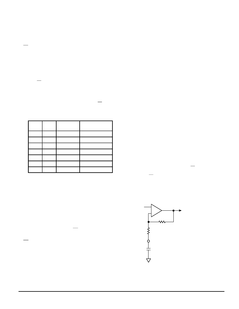
FB
Filter Bias (Pin 10)
This is the negative input to the ac amplifier. In normal op-
eration, this pin is connected to analog ground through a
0.1
μ
F bypass capacitor in order to cancel the input offset
voltage of the limiter. It has a nominal input impedance of
16 k
. (see Figure 3).
SQT
Transmit Squelch (Pin 14)
When this input pin is at a logic high level, the modulator is
disabled. The line driver remains active if LB is at a logic low
level (see Table 2) .
When both LB and SQT are connected to a logic high
level, see Table 2, the entire chip is in a power down state
and all circuitry except the crystal oscillator is disabled. Total
power supply current decreases from 10 mA (Max) to 300
μ
A
(Max).
0.1
μ
F
FB
16 k
10
490 k
+
–
FROM
BAND–PASS
FILTER
TO
CARRIER DETECT CIRCUIT
AND DEMODULATOR
Figure 3. ac Amplifier Circuit
相關(guān)PDF資料 |
PDF描述 |
|---|---|
| MC145443 | Single-Chip 300-Baud Modem |
| MC145442P | Single-Chip 300-Baud Modem |
| MC145443DW | Single-Chip 300-Baud Modem |
| MC145443P | Single-Chip 300-Baud Modem |
| MC145444DW | Single-Chip 300-Baud Modem |
相關(guān)代理商/技術(shù)參數(shù) |
參數(shù)描述 |
|---|---|
| MC145443P | 制造商:Motorola Inc 功能描述: |
| MC145446AFW | 制造商:Rochester Electronics LLC 功能描述:- Bulk 制造商:Motorola Inc 功能描述: 制造商:MOTOROLA 功能描述: |
| MC145447DW | 制造商:Motorola Inc 功能描述:CALLER NUMBER ID CIRCUIT, 16 Pin, Plastic, SOP |
| MC145447DWR2 | 制造商:Motorola Inc 功能描述:TELEPHONE MULTIFUNCTION CKT, 16 Pin Plastic SOP |
| MC145447P | 制造商:Motorola Inc 功能描述: |
發(fā)布緊急采購,3分鐘左右您將得到回復。