- 您現(xiàn)在的位置:買賣IC網(wǎng) > PDF目錄10713 > MC1413PG (ON Semiconductor)IC TRANS ARRAY DARL HV 16DIP PDF資料下載
參數(shù)資料
| 型號: | MC1413PG |
| 廠商: | ON Semiconductor |
| 文件頁數(shù): | 4/8頁 |
| 文件大?。?/td> | 0K |
| 描述: | IC TRANS ARRAY DARL HV 16DIP |
| 標準包裝: | 25 |
| 類型: | 達林頓晶體管矩陣 |
| 驅動器/接收器數(shù): | 7/0 |
| 電源電壓: | 5V |
| 安裝類型: | 通孔 |
| 封裝/外殼: | 16-DIP(0.300",7.62mm) |
| 供應商設備封裝: | 16-DIP |
| 包裝: | 管件 |
| 產(chǎn)品目錄頁面: | 1129 (CN2011-ZH PDF) |
| 其它名稱: | MC1413PGOS |
MC1413, MC1413B, NCV1413B
http://onsemi.com
4
1 Output Conducting at a Time
PIN 10
All Types
1
% DUTY CYCLE
VI, INPUT VOLTAGE (V)
VCE(sat), SATURATION VOLTAGE (V)
100
1000
700
500
300
3
10
2
4
5
6
200
100
70
50
30
20
1.0
2.5
2.0
1.5
1.0
0.5
0
7
7.0
4.0
5.0
8.0
3.0
6.0
2.0
0
100
200
400
300
500
700
600
0.4
0.6
0.8
1.0
1.2
1.4
800
1.6
0
0.2
I C
,COLLECT
OR
CURRENT
(mA)
I I
,INPUT
CURRENT
(mA)
I C
,COLLECT
OR
CURRENT
(mA)
NUMBER
OF
DRIVERS
USED
PIN 13
All Types
100
400
300
350
250
200
150
100
400
0
300
200
0
II, INPUT CURRENT (mA)
50
I O
,OUTPUT
CURRENT
(mA)
TYPICAL PERFORMANCE CURVES TA = 25°C
VI, INPUT VOLTAGE (V)
0
1.0
2.0
3.0
4.0
5.0
10
9.0
8.0
11
12
400
300
200
100
0
I O
,OUTPUT
CURRENT
(mA)
MC1413, B
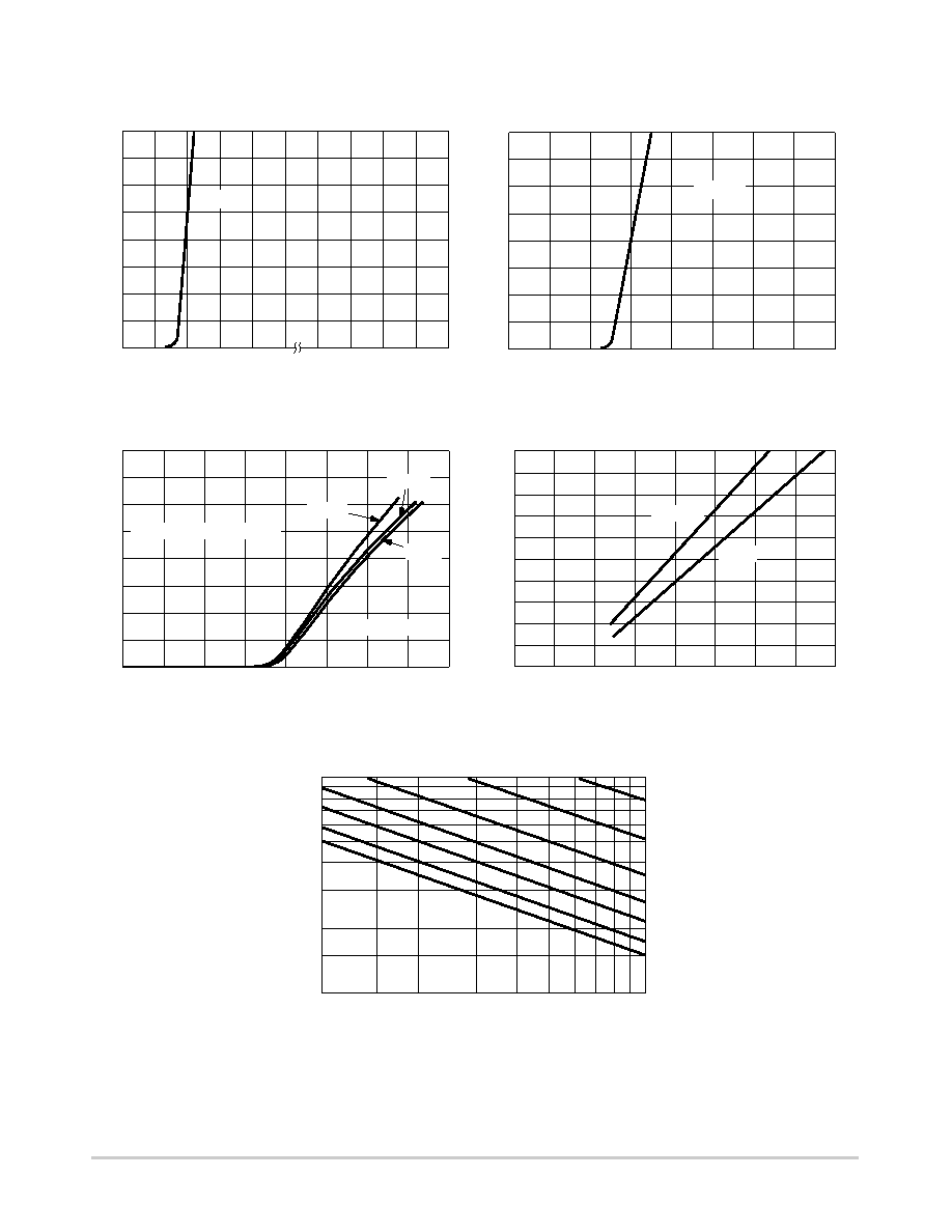
Figure 3. Output Current versus Input Voltage
Figure 4. Output Current versus Input Current
Figure 5. Typical Output Characteristics
Figure 6. Input Characteristics MC1413, B
Figure 7. Maximum Collector Current
versus Duty Cycle
(and Number of Drivers in Use)
PIN 16
Maximum
Typical
相關PDF資料 |
PDF描述 |
|---|---|
| TLC2555ID | IC 12BIT 400 KSPS ADC S/O 8-SOIC |
| VI-21V-IX-B1 | CONVERTER MOD DC/DC 5.8V 75W |
| VI-21T-IX-B1 | CONVERTER MOD DC/DC 6.5V 75W |
| VE-21T-IX-B1 | CONVERTER MOD DC/DC 6.5V 75W |
| VE-21W-IX-B1 | CONVERTER MOD DC/DC 5.5V 75W |
相關代理商/技術參數(shù) |
參數(shù)描述 |
|---|---|
| MC1414 | 制造商:Panasonic Industrial Company 功能描述:IC |
| MC141540 | 制造商:Panasonic Industrial Company 功能描述:IC |
| MC141540P4 | 制造商:Panasonic Industrial Company 功能描述:IC |
| MC141541P | 制造商:Panasonic Industrial Company 功能描述:IC |
| MC141542P2A | 制造商:Freescale Semiconductor 功能描述:GRAPHIC MONITOR - Rail/Tube |
發(fā)布緊急采購,3分鐘左右您將得到回復。