- 您現(xiàn)在的位置:買賣IC網(wǎng) > PDF目錄378657 > MC1377DW (MOTOROLA INC) COLOR TELEVISION RGB to PAL/NTSC ENCODER PDF資料下載
參數(shù)資料
| 型號(hào): | MC1377DW |
| 廠商: | MOTOROLA INC |
| 元件分類: | 顏色信號(hào)轉(zhuǎn)換 |
| 英文描述: | COLOR TELEVISION RGB to PAL/NTSC ENCODER |
| 中文描述: | COLOR SIGNAL ENCODER, PDSO20 |
| 封裝: | PLASTIC, SOIC-20 |
| 文件頁(yè)數(shù): | 5/18頁(yè) |
| 文件大小: | 643K |
| 代理商: | MC1377DW |
第1頁(yè)第2頁(yè)第3頁(yè)第4頁(yè)當(dāng)前第5頁(yè)第6頁(yè)第7頁(yè)第8頁(yè)第9頁(yè)第10頁(yè)第11頁(yè)第12頁(yè)第13頁(yè)第14頁(yè)第15頁(yè)第16頁(yè)第17頁(yè)第18頁(yè)
MC1377
5
MOTOROLA ANALOG IC DEVICE DATA
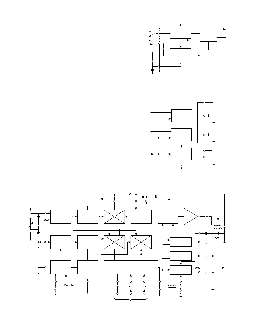
Timing Circuitry
The composite sync input at Pin 2 performs three
important functions: it provides the timing (but not the
amplitude) for the sync in the final output; it drives the black
level clamps in the modulators and output amplifier; and it
triggers the ramp generator at Pin 1, which produces burst
envelope and PAL switching. A representative block diagram
of the timing circuitry is shown in Figure 5.
In order to produce a color burst, a burst envelope must be
generated which “gates” a color subcarrier into the R–Y and
B–Y modulators. This is done with the ramp generator at
Pin 1.
The ramp generator at Pin 1 is an R–C type in which the
pin is held low until the arrival of the
leading
edge of sync. The
rising ramp function, with time constant R–C, passes through
two level sensors – the first one starts the gating pulse and
the second stops it (see Figure 10). Since the “early” part of
the exponential is used, the timing provided is relatively
accurate from chip–to–chip and assembly–to–assembly.
Fixed components are usually adequate. The ramp
continues to rise for more than half of the line interval, thereby
inhibiting burst generation on “half interval” pulses on vertical
front and back porches. The ramp method will produce burst
on the vertical front and back “porches” at full line intervals.
R–Y, B–Y Clamps and Output Clamp/Amplifier
The sync signal, shown in the block diagram of Figure 6,
drives the R–Y and B–Y clamps which clamp the R–Y and
B–Y signals to reference black during the blanking periods.
The output amplifier/clamp provides this same function plus
combines and amplifies the chroma and luma components
for composite video output.
Application Circuit
Figure 7 illustrates the block diagram of the MC1377 and
the external circuitry required for typical operation.
11
Sync
Input
Figure 5. Timing Circuitry
Figure 6. R–Y, B–Y and Output Amplifier Clamps
PAL/
NTSC
H/2
Line Drive
10k
Latching
Ramp
Generator
Dual
Comparator
Burst Flag
Burst
Pulse
Driver
PAL/NTSC
Control
20
2
1
B–Y
R–Y
Sync
B–Y
Clamp
R–Y
Clamp
Output
Amp/Clamp
Chroma
10
12
9
7
8
–Y
Composite
Video
VB
R
C
0.1
0.1
0.01
Figure 7. Block Diagram and Application Circuit
VCC
R–Y
B–Y
Osc/
Buffer
Voltage
Controlled
90
°
8.2V
Regulator
PAL
Switch
0/180
°
Chroma
Amp
B–Y
Clamp
R–Y
Clamp
Output Amp/
Clamp
Color Difference and
Luminance Matrix
Dual
Comparator
Latching
Ramp
Gen
PAL/NTS
C
Control
Burst
Pulse
Driver
0.01
19
16
VB
0.1
TOKO 166NNF
–10264AG
13
220
100/
62*
0.1
3.3k
47/33*
10
9
70.01
12
0.1
0.1
1000
3.58/
4.43*
MHz
220
220
5.0 to
25pF
20
15
1
2
3
4
5
6
8
56k
0.001
mica
Composite
Sync
Input
14
11
Composite
Video Output
1.0k
400ns
Y Delay
1.0k
+
+
+
15
μ
F
15
μ
F
15
μ
F
VB
R
G
B
R, G, B Inputs
H/2
90
°
0
°
NTSC/
PAL Select
17
18
* Refers to the choice NTSC/PAL
*
(3.58 MHz/4.43 MHz).
R–Y
B–Y
–Y
–Y
相關(guān)PDF資料 |
PDF描述 |
|---|---|
| MC1377P | COLOR TELEVISION RGB to PAL/NTSC ENCODER |
| MC1378FN | COLOR TELEVISION COMPOSITE VIDEO OVERLAY SYNCHRONIZER |
| MC1378P | COLOR TELEVISION COMPOSITE VIDEO OVERLAY SYNCHRONIZER |
| MC141539T1R | LCD Segment / Common Driver with Controller CMOS |
| MC141539T2R | LCD Segment / Common Driver with Controller CMOS |
相關(guān)代理商/技術(shù)參數(shù) |
參數(shù)描述 |
|---|---|
| MC1377P | 制造商:Motorola Inc 功能描述: |
| MC1378 | 制造商:MOTOROLA 制造商全稱:Motorola, Inc 功能描述:COLOR TELEVISION COMPOSITE VIDEO OVERLAY SYNCHRONIZER |
| MC13783 | 制造商:FREESCALE 制造商全稱:Freescale Semiconductor, Inc 功能描述:Power Management and Audio Circuit |
| MC13783_09 | 制造商:FREESCALE 制造商全稱:Freescale Semiconductor, Inc 功能描述:Power Management and Audio Circuit |
| MC13783JVK5 | 功能描述:接口—CODEC ATLAS 3G PWRMNGMNT 5 RoHS:否 制造商:Texas Instruments 類型: 分辨率: 轉(zhuǎn)換速率:48 kSPs 接口類型:I2C ADC 數(shù)量:2 DAC 數(shù)量:4 工作電源電壓:1.8 V, 2.1 V, 2.3 V to 5.5 V 最大工作溫度:+ 85 C 安裝風(fēng)格:SMD/SMT 封裝 / 箱體:DSBGA-81 封裝:Reel |
發(fā)布緊急采購(gòu),3分鐘左右您將得到回復(fù)。