- 您現(xiàn)在的位置:買賣IC網(wǎng) > PDF目錄371009 > MC1374 (Motorola, Inc.) TV MODULATOR CIRCUIT PDF資料下載
參數(shù)資料
| 型號: | MC1374 |
| 廠商: | Motorola, Inc. |
| 英文描述: | TV MODULATOR CIRCUIT |
| 中文描述: | 電視調(diào)制電路 |
| 文件頁數(shù): | 6/10頁 |
| 文件大?。?/td> | 122K |
| 代理商: | MC1374 |

MC1374
6
MOTOROLA ANALOG IC DEVICE DATA
FM Section
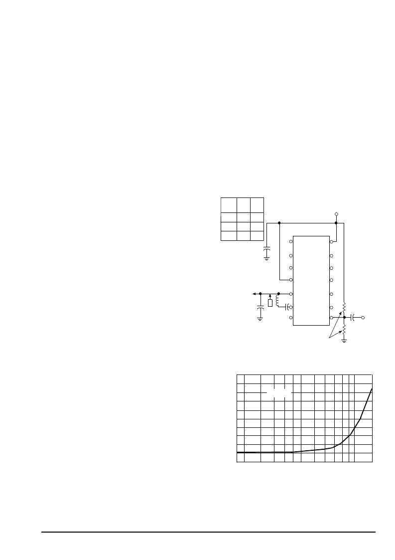
The oscillator center is approximately the resonance of the
inductor L2 from Pin 2 to Pin 3 and the effective capacitance
C3 from Pin 3 to ground. For overall oscillator stability, it is
best to keep XL in the range of 300
to 1.0 k
.
The modulator transfer characteristic at 4.5 MHz is shown
in Figure 15. Transfer curves at other frequencies have a very
similar shape, but differ in deviation per input volt, as shown in
Figures 13 and 17.
Most applications will not require DC connection to the
audio input, Pin 14. However, some improvements can be
achieved by the addition of biasing circuitry. The unaided
device will establish its own Pin 14 bias at 4
θ
, or about 3.0 V.
This bias is a little too high for optimum modulation linearity.
Figure 14 shows better than 2 to 1 improvement in distortion
between the unaided device and pulling Pin 14 down to 2.6 V
to 2.7 V. This can be accomplished by a simple divider, if the
supply voltage is relatively constant.
The impedance of the divider has a bearing on the
frequency versus temperature stability of the FM system. A
divider of 180 k
and 30 k
(for VCC = 12 V) will give good
temperature stabilization results. However, as Figure 18
shows, a divider is not a good method if the supply voltage
varies. The designer must make the decisions here, based
on considerations of economy, distortion and temperature
requirements and power supply capability. If the distortion
requirements are not stringent, then no bias components are
needed. If, in this case, the temperature compensation needs
to be improved in the high ambient area, the tuning capacitor
from Pin 3 to ground can be selected from N75 or N150
temperature compensation types.
Another reason for DC input to Pin 14 is the possibility of
automatic frequency control. Where high accuracy of
inter–carrier frequency is required, it may be desirable to feed
back the DC output of an AFC or phase detector for nominal
carrier frequency control. Only limited control range could be
used without adversely affecting the distortion performance,
but very little frequency compensation will be needed.
One added convenience in the FM section is the separate
Pin “oscillator B+” which permits disabling of the sound
system during alignment of the AM section. Usually it can be
hard wired to the VCC source without decoupling.
Standard practice in television is to provide pre–emphasis
of higher audio frequencies at the transmitter and a matching
de–emphasis in the TV receiver audio amplifier. The purpose
of this is to counteract the fact that less energy is usually
present in the higher frequencies, and also that fewer
modulation sidebands are within the deviation window. Both
factors degrade signal to noise ration. Pre–emphasis of 75
μ
s
is standard practice. For cases where it has not been
provided, a suitable pre–emphasis network is covered in
Figure 20.
It would seem natural to take the FM system output from
Pin 2, the emitter follower output, but this output is high in
harmonic content. Taking the output from Pin 3 sacrifices
somewhat in source impedance but results in a clean output
fundamental, with all harmonics more than 40 dB down. This
choice removes the need for additional filtering components.
The source impedance of Pin 3 is approximately 2.0 k
, and
the open circuit amplitude is about 900 mV pp for the test
circuit shown in Figure 11.
The application circuit of Figure 1 shows the
recommended approach to coupling the FM output from Pin 3
to the AM modulator input, Pin 1. The input impedance at Pin
1 is very high, so the intercarrier level is determined by the
source impedance of Pin 3 driving through C4 into the video
bias circuit impedance of R4 and R5, about 2.2 k. This
provides an intercarrier level of 500 mV pp, which is correct
for the 1.0 V peak video level chosen in this design. Resistor
R6 and the input capacitance of Pin 1 provide some
decoupling of stray pickup of RF oscillator or AM output which
may be coupled to the sound circuitry.
C3
(pF)
fo
(MHz)
L2
(μ
H)
10.7
12
10
4.5
120
10
40
200
1.76
VCC
C14
0.01
μ
F
Intercarrier
Sound Output
(Use FET Probe)
L2
10
μ
H
C3
120pF
C5
0.001
μ
F
7
6
5
4
3
2
1
8
9
10
11
12
13
14
R12
+
R13
Audio
Input
C6
1
μ
F
Optional Bias R
(See Text)
Figure 11. FM Test Circuit
1.4
2.0
3.0
5.0
4.0
6.0 7.0 8.09.0 10
14
fosc, OSCILLATOR FREQUENCY [MHz]
M
S
TA = 25
°
C
Figure 12. Modulator Sensitivity
2.0
1.8
1.6
1.4
1.2
1.0
0.8
0.6
0.4
0.2
0
相關(guān)PDF資料 |
PDF描述 |
|---|---|
| MC13751FCR2 | DUAL-BAND UPMIXER AND DRIVER AMPLIFIER |
| MC13760 | GSM/DCS/TDMA/AMPS Multi-Protocol Transceiver |
| MC1391P | TV HORIZONTAL PROCESSOR |
| MC1391 | TV HORIZONTAL PROCESSOR |
| MC14001BCL | B-Suffix Series CMOS Gates |
相關(guān)代理商/技術(shù)參數(shù) |
參數(shù)描述 |
|---|---|
| MC13745 | 制造商:PRIVATE LABEL 功能描述:Tactile Switch, ON-OFF Action, Rated 50m |
| MC1374P | 制造商:MOTOROLA 制造商全稱:Motorola, Inc 功能描述:TV MODULATOR CIRCUIT |
| MC13751 | 制造商:MOTOROLA 制造商全稱:Motorola, Inc 功能描述:DUAL-BAND UPMIXER AND DRIVER AMPLIFIER |
| MC13751FCR2 | 制造商:MOTOROLA 制造商全稱:Motorola, Inc 功能描述:DUAL-BAND UPMIXER AND DRIVER AMPLIFIER |
| MC13760 | 制造商:MOTOROLA 制造商全稱:Motorola, Inc 功能描述:GSM/DCS/TDMA/AMPS Multi-Protocol Transceiver |
發(fā)布緊急采購,3分鐘左右您將得到回復。