- 您現(xiàn)在的位置:買賣IC網(wǎng) > PDF目錄369894 > MC12430 (Motorola, Inc.) High Frequency PLL Clock Generator(高頻PLL時鐘發(fā)生器) PDF資料下載
參數(shù)資料
| 型號: | MC12430 |
| 廠商: | Motorola, Inc. |
| 英文描述: | High Frequency PLL Clock Generator(高頻PLL時鐘發(fā)生器) |
| 中文描述: | 高頻PLL時鐘發(fā)生器(高頻鎖相環(huán)時鐘發(fā)生器) |
| 文件頁數(shù): | 2/11頁 |
| 文件大小: | 127K |
| 代理商: | MC12430 |

MC12430
MOTOROLA
ECLinPS and ECLinPS Lite
DL140 — Rev 3
2
1
N[1]
N[0]
M[8]
M[7]
M[6]
M[5]
M[4]
XTAL1
XTAL_SEL
FREF_EXT
PLL–VCC
S_LOAD
S_DATA
S_CLOCK
4
3
2
28
27
26
25
24
23
22
21
20
19
18
17
16
15
14
13
12
11
10
9
7
8
6
5
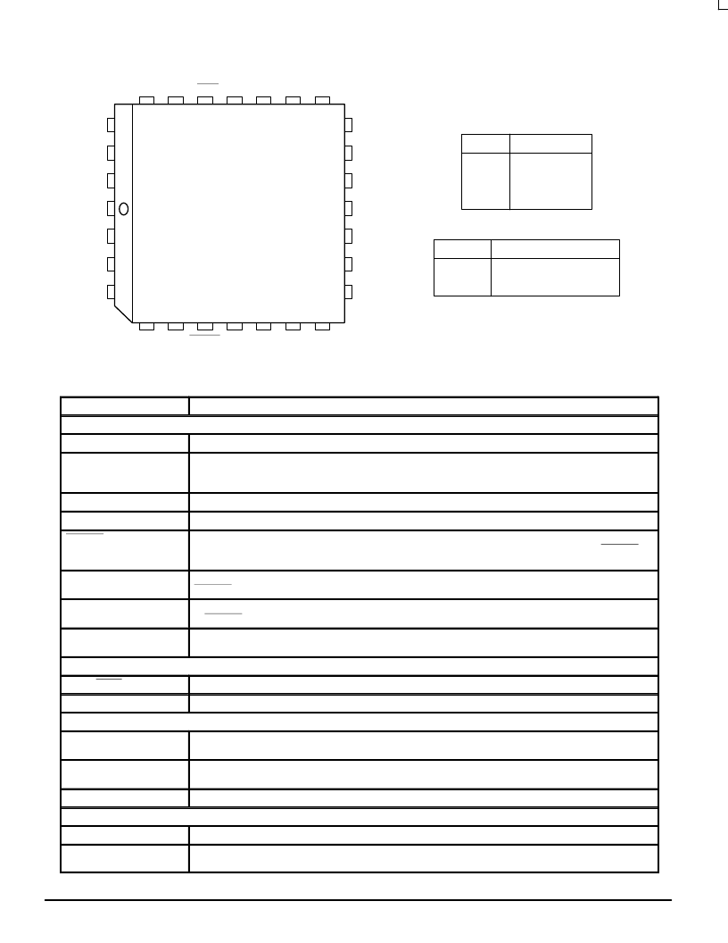
Figure 1. 28–Lead Pinout
(Top View)
P_LOAD
VCC
FOUT
FOUT GND
VCC
TEST GND
M[3]
M[2]
M[1]
M[0]
OE
XTAL2
N[1:0]
0 0
0 1
1 0
1 1
Output Division
2
4
8
1
Input
XTAL_SEL
OE
0
FREF_EXT
Disabled
1
XTAL
Enabled
PIN DESCRIPTIONS
Pin Name
Function
Inputs
XTAL1, XTAL2
These pins form an oscillator when connected to an external series–resonant crystal.
S_LOAD
(Int. Pulldown)
This pin loads the configuration latches with the contents of the shift registers. The latches will be transparent
when this signal is HIGH, thus the data must be stable on the HIGH–to–LOW transition of S_LOAD for proper
operation.
S_DATA
(Int. Pulldown)
This pin acts as the data input to the serial configuration shift registers.
S_CLOCK
(Int. Pulldown)
This pin serves to clock the serial configuration shift registers. Data from S_DATA is sampled on the rising edge.
P_LOAD
(Int. Pullup)
This pin loads the configuration latches with the contents of the parallel inputs .The latches will be transparent
when this signal is LOW, thus the parallel data must be stable on the LOW–to–HIGH transition of P_LOAD for
proper operation.
M[8:0]
(Int. Pullup)
These pins are used to configure the PLL loop divider. They are sampled on the LOW–to–HIGH transition of
P_LOAD. M[8] is the MSB, M[0] is the LSB.
N[1:0]
(Int. Pullup)
These pins are used to configure the output divider modulus. They are sampled on the LOW–to–HIGH transition
of P_LOAD.
OE
(Int. Pullup)
Active HIGH Output Enable. The Enable is synchronous to eliminate possibility of runt pulse generation on the
FOUT output.
Outputs
FOUT, FOUT
These differential positive–referenced ECL signals (PECL) are the output of the synthesizer.
TEST
The function of this output is determined by the serial configuration bits T[2:0]. The output is single–ended ECL.
Power
VCC
This is the positive supply for the internal logic and the output buffer of the chip, and is connected to +3.3V or
5.0V (VCC = PLL_VCC). Current drain through VCC
≈
85mA.
This is the positive supply for the PLL, and should be as noise–free as possible for low–jitter operation. This
supply is connected to +3.3V or 5.0V (VCC = PLL_VCC). Current drain through PLL_VCC
≈
15mA.
PLL_VCC
GND
These pins are the negative supply for the chip and are normally all connected to ground.
Other
FREF_EXT (Int. Pulldown)
LVCMOS/CMOS input which can be used as the PLL reference.
XTAL_SEL
(Int. Pullup)
LVCMOS/CMOS input that selects between the crystal and the FREF_EXT source for the PLL reference signal.
A HIGH selects the crystal input.
相關PDF資料 |
PDF描述 |
|---|---|
| MC13025 | Electronically Tuned Radio Front End |
| MC13028A | C-QUAM AM STEREO ADVANCED WIDE VOLTAGE IF and DECODER for E.T.R. RADIOS |
| MC13109 | Universal Cordless Telephone Subsystem IC |
| MC13109FB | Universal Cordless Telephone Subsystem IC |
| MC13109FTA | Universal Cordless Telephone Subsystem IC |
相關代理商/技術參數(shù) |
參數(shù)描述 |
|---|---|
| MC12430FA | 制造商:MOTOROLA 制造商全稱:Motorola, Inc 功能描述:HIGH FREQUENCY PLL CLOCK GENERATOR |
| MC12430FN | 制造商:MOTOROLA 制造商全稱:Motorola, Inc 功能描述:HIGH FREQUENCY PLL CLOCK GENERATOR |
| MC12439 | 制造商:MOTOROLA 制造商全稱:Motorola, Inc 功能描述:HIGH FREQUENCY PLL CLOCK GENERATOR |
| MC12439FN | 制造商:Motorola Inc 功能描述: 制造商:Motorola Inc 功能描述:MISCELLANEOUS CLOCK GENERATOR, 28 Pin, Plastic, PLCC |
| MC1243F | 制造商:Rochester Electronics LLC 功能描述:- Bulk |
發(fā)布緊急采購,3分鐘左右您將得到回復。