- 您現(xiàn)在的位置:買賣IC網(wǎng) > PDF目錄369894 > MC12181 (Motorola, Inc.) 125 -1000MHZ Frequency Synthesizer(125 -1000MHZ頻率合成器) PDF資料下載
參數(shù)資料
| 型號: | MC12181 |
| 廠商: | Motorola, Inc. |
| 英文描述: | 125 -1000MHZ Frequency Synthesizer(125 -1000MHZ頻率合成器) |
| 中文描述: | 125 - 1000MHz的頻率合成器(125 - 1000MHz的頻率合成器) |
| 文件頁數(shù): | 7/9頁 |
| 文件大?。?/td> | 110K |
| 代理商: | MC12181 |

MC12181
7
MOTOROLA RF/IF DEVICE DATA
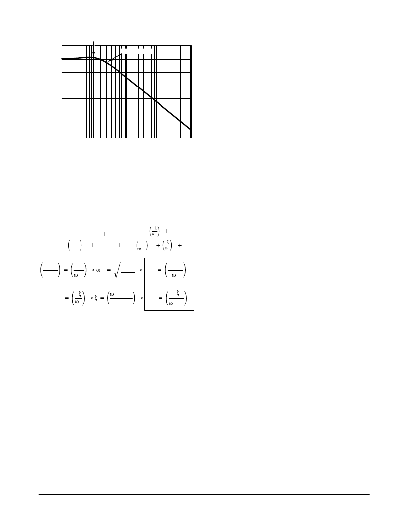
Figure 8. Closed Loop Frequency Response for
ζ
= 1
Natural Frequency
–60
–50
–40
–30
–20
–10
0
10
0.1
1.0 k
Hz
d
1.0
10
100
3dB Bandwidth
To simplify analysis further a damping factor of 1 will be
selected. The normalized closed loop response is illustrated
in Figure 8 where the loop bandwidth is 2.5 times the loop
natural frequency (the loop natural frequency is the
frequency at which the loop would oscillate if it were
unstable). Therefore the optimum loop bandwidth is
15 kHz/2.5 or 6.0 kHz (37.7 krads) with a damping coefficient,
ζ
≈
1. T(s) is the transfer function of the loop filter.
T(s)
RoCos
1
NCo
KpKv
s2
RoCos
1
2
o
s
1
1
o2
s2
2
o
s
1
NCo
KpKv
1
o2
o
KpKv
NCo
Co
KpKv
N o2
RoCo
2
o
oRoCo
2
Ro
2
oCo
where Nt = Total PLL Divide Ratio — 8
×
N where (N = 25...40)
Kv = VCO Gain — Hz/V
Kp = Phase Detector/Charge Pump Gain — A
= ( |IOH| + |IOL| ) / 2
Technically, Kv and Kp should be expressed in Radian
units [Kv (RAD/V), Kp (A/RAD)]. Since the component
design equation contains the Kv
×
Kp term. the 2
π
cancels and the values can be epressed as above.
Figure 9. Design Equations for the 2nd Order System
In summary, follow the steps given below:
Step 1: Plot the phase noise of crystal reference and the
VCO on the same graph.
Step 2: Increase the phase noise of the crystal reference by
the noise contribution of the loop.
Step 3: Convert the divide–by–N to dB (20log 8
×
N) and
increase the phase noise of the crystal reference by
that amount.
Step 4: The point at which the VCO phase noise crosses the
amplified phase noise of the Crystal Reference is the
point of the optimum loop bandwidth. This is
approximately 15 kHz in Figure 7.
Step 5: Correlate this loop bandwidth to the loop natural
frequency per Figure 8. In this case the 3.0 dB
bandwidth for a damping coefficient of 1 is 2.5 times
the loop’s natural frequency. The relationship
between the 3.0 dB loop bandwidth and the loop’s
“natural” frequency will vary for different values of
ζ
.
Making use of the equations defined in Figure 9, a
math tool or spread sheet is useful to select the
values for Ro and Co.
Appendix: Derivation of Loop Filter Transfer Function
The purpose of the loop filter is to convert the current from
the phase detector to a tuning voltage for the VCO. The total
transfer function is derived in two steps. Step 1 is to find the
voltage generated by the impedance of the loop filter. Step 2
is to find the transfer function from the input of the loop filter to
its output. The “voltage” times the “transfer function” is the
overall transfer function of the loop filter. To use these
equations in determining the overall transfer function of a PLL
multiply the filter’s impedance by the gain constant of the
phase detector then multiply that by the filter’s transfer
function (Figure 10 contains the transfer function equations
for 2nd, 3rd and 4th order PLL filters.)
相關(guān)PDF資料 |
PDF描述 |
|---|---|
| MC12181D | 125 - 1000 MHZ FREQUENCY SYNTHESIZER |
| MC12429 | High Frequency PLL Clock Generator(高頻PLL時鐘發(fā)生器) |
| MC12430 | High Frequency PLL Clock Generator(高頻PLL時鐘發(fā)生器) |
| MC13025 | Electronically Tuned Radio Front End |
| MC13028A | C-QUAM AM STEREO ADVANCED WIDE VOLTAGE IF and DECODER for E.T.R. RADIOS |
相關(guān)代理商/技術(shù)參數(shù) |
參數(shù)描述 |
|---|---|
| MC12181D | 制造商:MOTOROLA 制造商全稱:Motorola, Inc 功能描述:125 - 1000 MHZ FREQUENCY SYNTHESIZER |
| MC1218F | 制造商:Rochester Electronics LLC 功能描述:- Bulk |
| MC1218L | 制造商:Rochester Electronics LLC 功能描述:- Bulk |
| MC-121EU | 制造商:Amphenol Aerospace 功能描述:HEADSET CONNECTOR 制造商:Amphenol Nexus 功能描述:HEADSET CONNECTOR - Bulk |
| MC-121SP | 制造商:Amphenol Nexus 功能描述:HEADSET CONNECTOR - Bulk |
發(fā)布緊急采購,3分鐘左右您將得到回復(fù)。