- 您現(xiàn)在的位置:買(mǎi)賣(mài)IC網(wǎng) > PDF目錄369894 > MC12179 (Motorola, Inc.) 500 - 2800 MHz Single Channel Frequency Synthesizer PDF資料下載
參數(shù)資料
| 型號(hào): | MC12179 |
| 廠商: | Motorola, Inc. |
| 英文描述: | 500 - 2800 MHz Single Channel Frequency Synthesizer |
| 中文描述: | 500 - 2800兆赫頻率合成器的單頻道 |
| 文件頁(yè)數(shù): | 3/11頁(yè) |
| 文件大?。?/td> | 353K |
| 代理商: | MC12179 |

3
MOTOROLA RF/IF DEVICE DATA
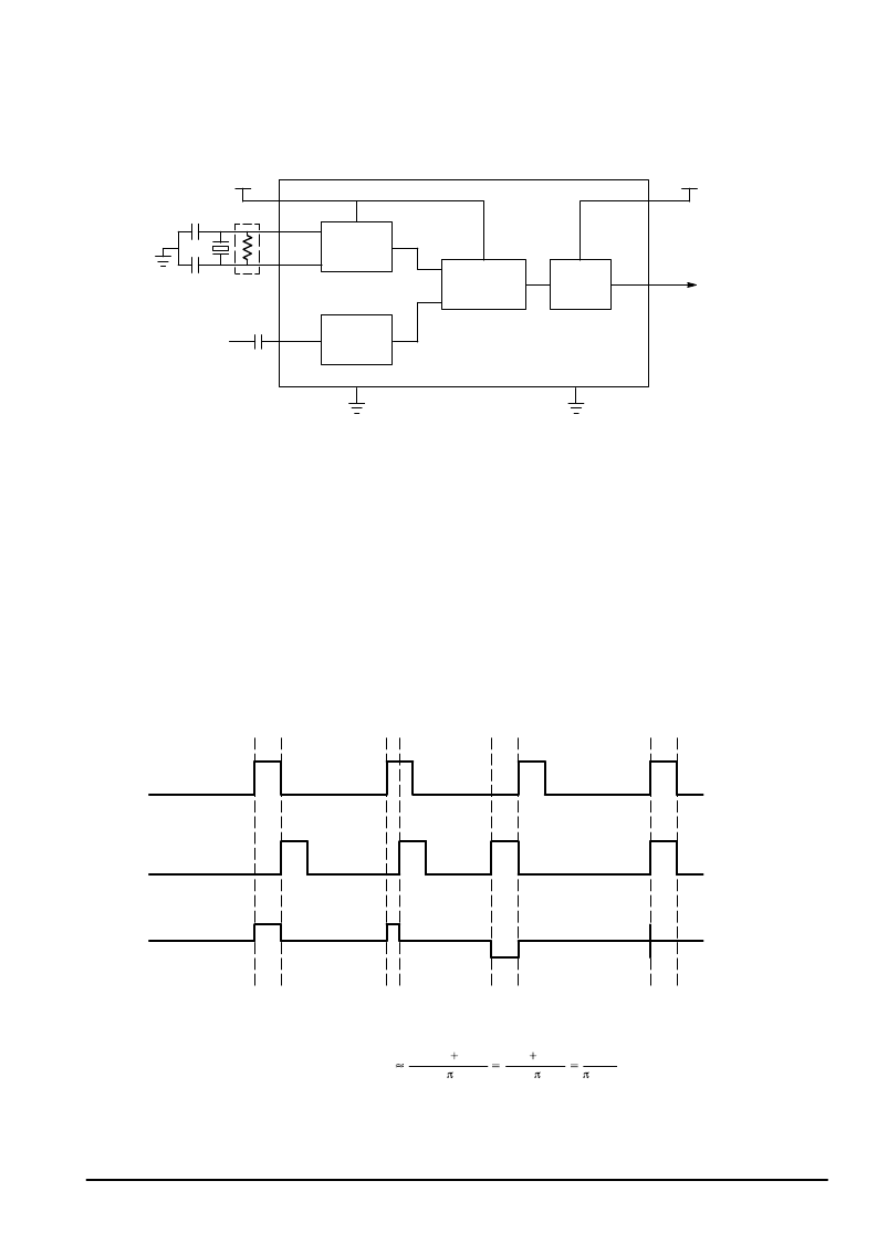
Figure 1. MC12179 Expanded Block Diagram
Crystal
Oscillator
Prescaler
÷
256
Phase/Frequency
Detector
Charge
Pump
VCC
OSCin
OSCout
2
1
8
4
C1
C2
VCO
+5.0 V
fr
fv
VP
7
+5.0 V
6
To Loop Filter
GND
GNDP
5
3
NOTE: External 50 k
resistor
across Pins 1 and 8 is necessary in
either crystal or driven mode.
1000 pF
Fin
PDout
PHASE CHARACTERISTICS
The phase comparator in the MC12179 is a high speed
digital phase/frequency detector circuit. The circuit
determines the “l(fā)ead” or “l(fā)ag” phase relationship and time
difference between the leading edges of the VCO (fv) signal
and the reference (fr) input. The detector can cover a range of
±
2
π
radian of fv/fr phase difference. The operation of the
charge pump output is shown in Figure 2.
fr lags fv in phase OR fv>fr in frequency
When the phase of fr lags that of fv or the frequency of fv is
greater than fr, the Do output will sink current. The pulse
width will be determined by the time difference between the
two rising edges.
fr leads fv in phase OR fv<fr in frequency
When the phase of fr leads that of fv or the frequency of fv
is less than fr, the Do output will source current. The pulse
width will be determined by the time difference between the
two rising edges.
fr = fv in phase and frequency
When the phase and frequency of fr and fv are equal, the
charge pump will be in a quiet state, except for current spikes
when signals are in phase. This situation indicates that the
loop is in lock and the phase comparator will maintain the
loop in its locked state.
Figure 2. Phase/Frequency Detector and Charge Pump Waveforms
fr
(OSCin)
H
L
fv
(Fin
÷
256)
H
L
PDout
Sourcing Current Pulse
Z
Sinking Current Pulse
H = High voltage level; L = Low voltage level; Z = High impedance
NOTES: Phase difference detection range:
~
–2
π
to 2
π
Kp–Charge Pump Gain
|Isource|
|Isink|
4
|2.2|
|–2.2|
4
1.1 mA
radian
A
A
F
Freescale Semiconductor, Inc.
For More Information On This Product,
Go to: www.freescale.com
n
.
相關(guān)PDF資料 |
PDF描述 |
|---|---|
| MC12181 | 125 -1000MHZ Frequency Synthesizer(125 -1000MHZ頻率合成器) |
| MC12181D | 125 - 1000 MHZ FREQUENCY SYNTHESIZER |
| MC12429 | High Frequency PLL Clock Generator(高頻PLL時(shí)鐘發(fā)生器) |
| MC12430 | High Frequency PLL Clock Generator(高頻PLL時(shí)鐘發(fā)生器) |
| MC13025 | Electronically Tuned Radio Front End |
相關(guān)代理商/技術(shù)參數(shù) |
參數(shù)描述 |
|---|---|
| MC12179D | 制造商:MOTOROLA 制造商全稱(chēng):Motorola, Inc 功能描述:500 - 2800 MHz SINGLE CHANNEL FREQUENCY SYNTHESIZER |
| MC12181 | 制造商:MOTOROLA 制造商全稱(chēng):Motorola, Inc 功能描述:125 - 1000 MHZ FREQUENCY SYNTHESIZER |
| MC12181D | 制造商:MOTOROLA 制造商全稱(chēng):Motorola, Inc 功能描述:125 - 1000 MHZ FREQUENCY SYNTHESIZER |
| MC1218F | 制造商:Rochester Electronics LLC 功能描述:- Bulk |
| MC1218L | 制造商:Rochester Electronics LLC 功能描述:- Bulk |
發(fā)布緊急采購(gòu),3分鐘左右您將得到回復(fù)。