- 您現(xiàn)在的位置:買賣IC網(wǎng) > PDF目錄369894 > MC12061P (MOTOROLA INC) CRYSTAL OSCILLATOR PDF資料下載
參數(shù)資料
| 型號: | MC12061P |
| 廠商: | MOTOROLA INC |
| 元件分類: | XO, clock |
| 英文描述: | CRYSTAL OSCILLATOR |
| 中文描述: | OTHER CLOCK GENERATOR, PDIP16 |
| 封裝: | PLASTIC, DIP-16 |
| 文件頁數(shù): | 6/9頁 |
| 文件大?。?/td> | 155K |
| 代理商: | MC12061P |

MC12061
6
MOTOROLA RF/IF DEVICE DATA
OPERATING CHARACTERISTICS
The MC12061 consists of three basic sections: an
oscillator with AGC and two translators (NO TAG). Buffered
complementary sine wave outputs are available from the
oscillator section. The translators convert these sine wave
outputs to levels compatible with MECL and/or TTL.
Series mode crystals should be used with the oscillator. If
it is necessary or desirable to adjust the crystal frequency, a
reactive element can be inserted in series with the crystal —
an inductor to lower the frequency or a capacitor to raise it.
When such an adjustment is necessary, it is recommended
that the crystal be specified slightly lower in frequency and a
series trimmer capacitor be added to bring the oscillator back
on frequency. As the oscillator frequency is changed from the
natural resonance of the crystal, more and more dependence
is placed on the external reactance, and temperature drift of
the trimming components then affects overall oscillator
performance.
The MC12061 is designed to operate from a single
supply — either +5.0 Vdc or –5.2 Vdc. Although each
translator has separate VCC and VEE supply pins, the
circuit is NOT designed to operate from both voltage levels
at the same time. The separate VEE pin from the TTL
translator helps minimize transient disturbance. If neither
translator is being used, all unused pins (9 thru 16) should
be connected to VEE (pin 8). With the translators not
powered, supply current drain is typically reduced from 42
mA to 23 mA for the MC12061.
Frequency Stability
Output frequency of different oscillator circuits (of a
given device type number) will vary somewhat when used
with a given test setup. However, the variation should be
within approximately
±
0.001% from unit to unit.
Frequency variations with temperature (independent of
the crystal, which is held at 25
°
C) are small — about –0.08
ppm/
°
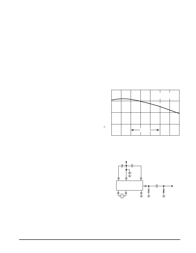
C for MC12061 operating at 8.0 MHz (see NO TAG).
Signal Characteristics
The sine wave outputs at either pin 2 or pin 3 will
typically range from 800 mVp-p (no load) to 500 mVp-p
(120 ohm ac load). Approximately 500 mVp-p can be
provided across 50 ohms by slightly increasing the dc
current in the output buffer by the addition of an external
resistor (680 ohms) from pin 2 or 3 to ground, as shown in
Figure 9. Frequency drift is typically less than 0.0003%
when going from a high-impedance load (1 megohm, 15
pF) to the 50 ohm load of Figure 9. The dc voltage level at
pin 2 or 3 is nominally 3.5 Vdc with VCC = +5.0 Vdc.
Harmonic distortion content in the sine wave outputs is
crystal as well as circuit dependent. The largest harmonic
(third) will usually be at least 15 dB down from the
fundamental. The harmonic content is approximately load
independent except that the higher harmonic levels
(greater than the fifth) are increased when the MECL
translator is being driven.
Typically, the MECL outputs (pins 12 and 13) will drive up
to five gates, as defined in NO TAG, and the TTL output (pin
10) will drive up to ten gates, as defined in NO TAG.
Noise Characteristics
Noise level evaluation of the sine wave outputs using the
circuit of NO TAG, with operation at or 9.0 MHz, indicates
the following characteristics:
1. Noise floor (200 kHz from oscillator center frequency) is
approximately –122 dB when referenced to a 1.0 Hz
bandwidth. Noise floor is not sensitive to load
conditions and/or translator operation.
2. Close-in noise (100 Hz from oscillator center frequency)
is approximately –88 dB when referenced to a 1.0 Hz
bandwidth.
+5.0 V
0.1
μ
F
0.1
μ
F
0.1
μ
F
4
7
1
2 or 3
0.1
μ
F
6
5
8
680
50
* See text under signal characteristics.
TA, AMBIENT TEMPERATURE (
°
)
+10
0
–10
–20
–30
–55
–25
0
25
50
75
100
125
f
Figure 8. Frequency Variation Due to Temperature
MC12061
VCC = +5.0 Vdc
Tcrystal = 25
°
C
MC12061
Figure 9. Driving Low Impedance Loads
相關PDF資料 |
PDF描述 |
|---|---|
| MC12061 | CRYSTAL OSCILLATOR |
| MC12089P | MECL PLL COMPONENTS ±64/128 PRESCALER |
| MC12089 | MECL PLL COMPONENTS ±64/128 PRESCALER |
| MC12089D | MECL PLL COMPONENTS ±64/128 PRESCALER |
| MC12100 | 200 MHz VOLTAGE CONTROLLED MULTIVIBRATOR |
相關代理商/技術參數(shù) |
參數(shù)描述 |
|---|---|
| MC1206-1R00-FTW | 制造商:RCD Components Inc 功能描述:Res Thick Film 1206 1 Ohm 1% 0.25W(1/4W) ±400ppm/°C Molded SMD T/R |
| MC1206-1R0-JTW | 制造商:RCD Components Inc 功能描述:Res Thick Film 1206 1 Ohm 5% 0.25W(1/4W) ±400ppm/°C Molded SMD T/R |
| MC1206-1R1-JTW | 制造商:RCD Components Inc 功能描述:CHIP RES 1206 1.1 OHM 5% T&R |
| MC1206-1R2-JTW | 制造商:RCD Components Inc 功能描述:CHIP RES 1206 1.2 OHM 5% T&R |
| MC1206-1R3-JTW | 制造商:RCD Components Inc 功能描述:CHIP RES 1206 1.3 OHM 5% T&R |
發(fā)布緊急采購,3分鐘左右您將得到回復。