- 您現(xiàn)在的位置:買賣IC網(wǎng) > PDF目錄377929 > MB90F822A (Fujitsu Limited) 16-bit Proprietary Microcontroller PDF資料下載
參數(shù)資料
| 型號: | MB90F822A |
| 廠商: | Fujitsu Limited |
| 英文描述: | 16-bit Proprietary Microcontroller |
| 中文描述: | 16位微控制器專有 |
| 文件頁數(shù): | 16/100頁 |
| 文件大?。?/td> | 992K |
| 代理商: | MB90F822A |
第1頁第2頁第3頁第4頁第5頁第6頁第7頁第8頁第9頁第10頁第11頁第12頁第13頁第14頁第15頁當前第16頁第17頁第18頁第19頁第20頁第21頁第22頁第23頁第24頁第25頁第26頁第27頁第28頁第29頁第30頁第31頁第32頁第33頁第34頁第35頁第36頁第37頁第38頁第39頁第40頁第41頁第42頁第43頁第44頁第45頁第46頁第47頁第48頁第49頁第50頁第51頁第52頁第53頁第54頁第55頁第56頁第57頁第58頁第59頁第60頁第61頁第62頁第63頁第64頁第65頁第66頁第67頁第68頁第69頁第70頁第71頁第72頁第73頁第74頁第75頁第76頁第77頁第78頁第79頁第80頁第81頁第82頁第83頁第84頁第85頁第86頁第87頁第88頁第89頁第90頁第91頁第92頁第93頁第94頁第95頁第96頁第97頁第98頁第99頁第100頁
MB90820 Series
16
5.
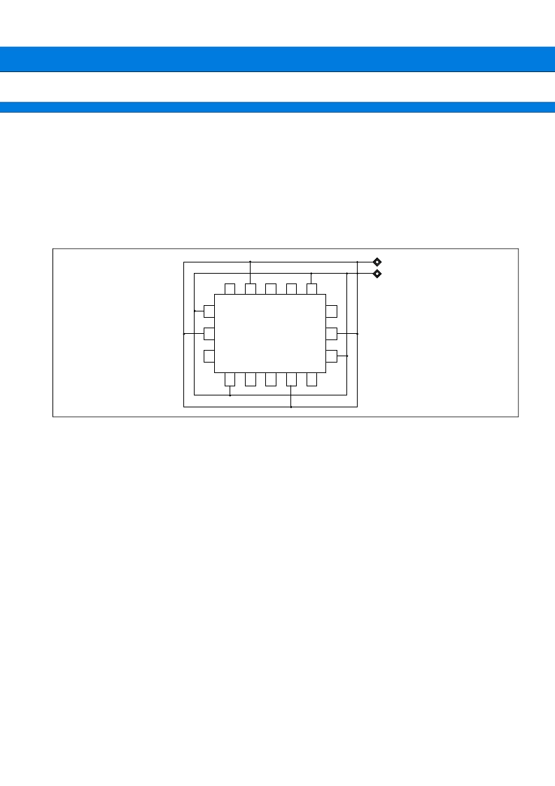
Power supply pins (V
CC
/V
SS
)
If there are multiple V
CC
and V
SS
pins, from the point of view of device design, pins to be of the same potential
are connected the inside of the device to prevent such malfunctioning as latch up.
To reduce unnecessary radiation, prevent malfunctioning of the strobe signal due to the rise of ground level,
and observe the standard for total output current, be sure to connect the V
CC
and V
SS
pins to the power supply
and ground externally.
Connect V
CC
and V
SS
to the device from the current supply source at a low impedance.
As a measure against power supply noise, connect a capacitor of about 0.1
μ
F as a bypass capacitor between
V
CC
and V
SS
in the vicinity of V
CC
and V
SS
pins of the device.
6.
Pull-up/pull-down resistors
The MB90820 series does not support internal pull-up/pull-down resistors option (Port 0 to Port 3 : built-in pull-
up resistors) . Use external components where needed.
Crystal oscillator circuit
7.
Noises around X0 or X1 pins may be possible causes of abnormal operations. Make sure to provide bypass
capacitors via shortest distance from X0, X1 pins, crystal oscillator (or ceramic oscillator) and ground lines, and
make sure, to the utmost effort, that lines of oscillation circuit do not cross the lines of other circuits while you
design a printed circuit board.
It is highly recommended to provide a printed circuit board art work surrounding X0 and X1 pins with a ground
area for stabilizing the operation.
Turning-on sequence of power supply to A/D converter and D/A converter, and analog inputs
8.
Make sure to turn on the A/D converter power supply, D/A converter power supply (AV
CC
, AVRH, AVR) and analog
inputs (AN0 to AN15) after turning-on the digital power supply (V
CC
).
Turn-off the digital power after turning off the A/D converter power supply, D/A converter power supply, and
analog inputs. In this case, make sure that the voltage not exceed AVR or AV
CC
(turning on/off the analog and
digital power supplies simultaneously is acceptable).
Connection of unused pins of A/D converter and D/A converter if A/D converter and
D/A converter are unused
9.
Connect unused pins of A/D converter and D/A converter to AV
CC
= V
CC
, AV
SS
= AVRH = AVRL = V
SS
.
10. Notes on energization
To prevent the internal regulator circuit from malfunctioning, set the voltage rise time during energization at
50
μ
s or more (0.2 V to 2.7 V) .
V
CC
V
SS
V
CC
V
CC
V
CC
V
CC
V
SS
V
SS
V
SS
V
SS
MB90820
Series
相關PDF資料 |
PDF描述 |
|---|---|
| MB90F822APF | 16-bit Proprietary Microcontroller |
| MB90F822APFM | 16-bit Proprietary Microcontroller |
| MB90F822APFV | 16-bit Proprietary Microcontroller |
| MB90F823A | 16-bit Proprietary Microcontroller |
| MB90F823APF | 16-bit Proprietary Microcontroller |
相關代理商/技術參數(shù) |
參數(shù)描述 |
|---|---|
| MB90F867APFR-G-SNE1 | 制造商:FUJITSU 功能描述: |
| MB90F867ASPF-GE1 | 制造商:FUJITSU 功能描述:IC 16BIT MCU I2C SMD QFP100 |
| MB90F867ASPFR-GE1 | 制造商:FUJITSU 功能描述: |
| MB90F867ASPFR-G-SPE1 | 制造商:FUJITSU 功能描述: |
| MB90F897PMCR-G-TE1 | 制造商:FUJITSU 功能描述: |
發(fā)布緊急采購,3分鐘左右您將得到回復。