- 您現(xiàn)在的位置:買(mǎi)賣(mài)IC網(wǎng) > PDF目錄377928 > MB90F583CA (Fujitsu Limited) 16-bit Proprietary Microcontroller PDF資料下載
參數(shù)資料
| 型號(hào): | MB90F583CA |
| 廠商: | Fujitsu Limited |
| 英文描述: | 16-bit Proprietary Microcontroller |
| 中文描述: | 16位微控制器專有 |
| 文件頁(yè)數(shù): | 19/124頁(yè) |
| 文件大?。?/td> | 2639K |
| 代理商: | MB90F583CA |
第1頁(yè)第2頁(yè)第3頁(yè)第4頁(yè)第5頁(yè)第6頁(yè)第7頁(yè)第8頁(yè)第9頁(yè)第10頁(yè)第11頁(yè)第12頁(yè)第13頁(yè)第14頁(yè)第15頁(yè)第16頁(yè)第17頁(yè)第18頁(yè)當(dāng)前第19頁(yè)第20頁(yè)第21頁(yè)第22頁(yè)第23頁(yè)第24頁(yè)第25頁(yè)第26頁(yè)第27頁(yè)第28頁(yè)第29頁(yè)第30頁(yè)第31頁(yè)第32頁(yè)第33頁(yè)第34頁(yè)第35頁(yè)第36頁(yè)第37頁(yè)第38頁(yè)第39頁(yè)第40頁(yè)第41頁(yè)第42頁(yè)第43頁(yè)第44頁(yè)第45頁(yè)第46頁(yè)第47頁(yè)第48頁(yè)第49頁(yè)第50頁(yè)第51頁(yè)第52頁(yè)第53頁(yè)第54頁(yè)第55頁(yè)第56頁(yè)第57頁(yè)第58頁(yè)第59頁(yè)第60頁(yè)第61頁(yè)第62頁(yè)第63頁(yè)第64頁(yè)第65頁(yè)第66頁(yè)第67頁(yè)第68頁(yè)第69頁(yè)第70頁(yè)第71頁(yè)第72頁(yè)第73頁(yè)第74頁(yè)第75頁(yè)第76頁(yè)第77頁(yè)第78頁(yè)第79頁(yè)第80頁(yè)第81頁(yè)第82頁(yè)第83頁(yè)第84頁(yè)第85頁(yè)第86頁(yè)第87頁(yè)第88頁(yè)第89頁(yè)第90頁(yè)第91頁(yè)第92頁(yè)第93頁(yè)第94頁(yè)第95頁(yè)第96頁(yè)第97頁(yè)第98頁(yè)第99頁(yè)第100頁(yè)第101頁(yè)第102頁(yè)第103頁(yè)第104頁(yè)第105頁(yè)第106頁(yè)第107頁(yè)第108頁(yè)第109頁(yè)第110頁(yè)第111頁(yè)第112頁(yè)第113頁(yè)第114頁(yè)第115頁(yè)第116頁(yè)第117頁(yè)第118頁(yè)第119頁(yè)第120頁(yè)第121頁(yè)第122頁(yè)第123頁(yè)第124頁(yè)
MB90580C Series
19
I
HANDLING DEVICES
1.
Preventing Latchup
CMOS ICs may cause latchup in the following situations:
When a voltage higher than Vcc or lower than Vss is applied to input or output pins.
When a voltage exceeding the rating is applied between Vcc and Vss.
When AVcc power is supplied prior to the Vcc voltage.
If latchup occurs, the power supply current increases rapidly, sometimes resulting in thermal breakdown of the
device. Use meticulous care not to let it occur.
For the same reason, also be careful not to let the analog power-supply voltage exceed the digital power-supply
voltage.
Handling unused input pins
2.
Unused input pins left open may cause abnormal operation, or latch-up leading to permanent damage. Unused
input pins should be pulled up or pulled down through at least 2 k
resistance.
Unused input/output pins may be left open in output state, but if such pins are in input state they should be
handled in the same way as input pins.
Treatment of the TX and RX pins with the IEBus
TM
unused
3.
When the IEBus is not used, connect a pull-down resistor to the TX pin and a pull-down/pull-up resistor to the
RX pin.
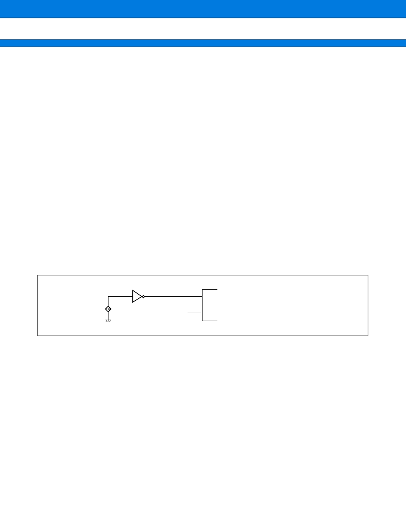
Use of the external clock
4.
When the device uses an external clock, drive only the X0 pin while leaving the X1 pin open (See the illustration
below).
5.
Power Supply Pins (V
CC
/V
SS
)
In products with multiple V
CC
or V
SS
pins, the pins of a same potential are internally connected in the device to
avoid abnormal operations including latch-up. However, connect the pins external power and ground lines to
lower the electro-magnetic emission level to prevent abnormal operation of strobe signals caused by the rise in
the ground level, and to conform to the total current rating.
Make sure to connect V
CC
and V
SS
pins via lowest impedance to power lines.
X0
X1
MB90580C series
Open
相關(guān)PDF資料 |
PDF描述 |
|---|---|
| MB90583C | Octal Bus Transceivers With 3-State Outputs 20-LCCC -55 to 125 |
| MB90F591GPF | 16-bit Proprietary Microcontroller |
| MB90F598 | 9-Bit Bus-Interface Flip-Flops With 3-State Outputs 24-CDIP -55 to 125 |
| MB90V595 | 16-bit Proprietary Microcontroller |
| MB90V595G | 16-bit Proprietary Microcontroller |
相關(guān)代理商/技術(shù)參數(shù) |
參數(shù)描述 |
|---|---|
| MB90F583CAPFR-GE1 | 制造商:FUJITSU 功能描述: |
| MB90F591GPFR-GE1 | 制造商:FUJITSU 功能描述: |
| MB90F594APFR-GE1 | 制造商:FUJITSU 功能描述: |
| MB90F594GPFR-GE1 | 制造商:FUJITSU 功能描述: |
| MB90F598GPFR-GE1 | 制造商:FUJITSU 功能描述: |
發(fā)布緊急采購(gòu),3分鐘左右您將得到回復(fù)。