- 您現(xiàn)在的位置:買賣IC網(wǎng) > PDF目錄377927 > MB90F574APMT (FUJITSU LTD) 16-bit Proprietary Microcontroller PDF資料下載
參數(shù)資料
| 型號: | MB90F574APMT |
| 廠商: | FUJITSU LTD |
| 元件分類: | 微控制器/微處理器 |
| 英文描述: | 16-bit Proprietary Microcontroller |
| 中文描述: | 16-BIT, FLASH, 16 MHz, MICROCONTROLLER, PQFP120 |
| 封裝: | 16 X 16 MM, 1.70 MM HEIGHT, 0.50 MM PITCH, PLASTIC, LQFP-120 |
| 文件頁數(shù): | 49/135頁 |
| 文件大小: | 2504K |
| 代理商: | MB90F574APMT |
第1頁第2頁第3頁第4頁第5頁第6頁第7頁第8頁第9頁第10頁第11頁第12頁第13頁第14頁第15頁第16頁第17頁第18頁第19頁第20頁第21頁第22頁第23頁第24頁第25頁第26頁第27頁第28頁第29頁第30頁第31頁第32頁第33頁第34頁第35頁第36頁第37頁第38頁第39頁第40頁第41頁第42頁第43頁第44頁第45頁第46頁第47頁第48頁當前第49頁第50頁第51頁第52頁第53頁第54頁第55頁第56頁第57頁第58頁第59頁第60頁第61頁第62頁第63頁第64頁第65頁第66頁第67頁第68頁第69頁第70頁第71頁第72頁第73頁第74頁第75頁第76頁第77頁第78頁第79頁第80頁第81頁第82頁第83頁第84頁第85頁第86頁第87頁第88頁第89頁第90頁第91頁第92頁第93頁第94頁第95頁第96頁第97頁第98頁第99頁第100頁第101頁第102頁第103頁第104頁第105頁第106頁第107頁第108頁第109頁第110頁第111頁第112頁第113頁第114頁第115頁第116頁第117頁第118頁第119頁第120頁第121頁第122頁第123頁第124頁第125頁第126頁第127頁第128頁第129頁第130頁第131頁第132頁第133頁第134頁第135頁
49
MB90570 Series
(3) Output Compare (OCU)
The output compare (OCU) is two sets of compare units consisting of four-channel OCU compare registers, a
comparator and a control register.
An interrupt request can be generated for each channel upon a match detection by performing time-division
comparison between the OCU compare data register setting value and the counter value of the 16-bit free run
timer.
The OUT pin can be used as a waveform output pin for reversing output upon a match detection or a general-
purpose output port for directly outputting the setting value of the CMOD bit.
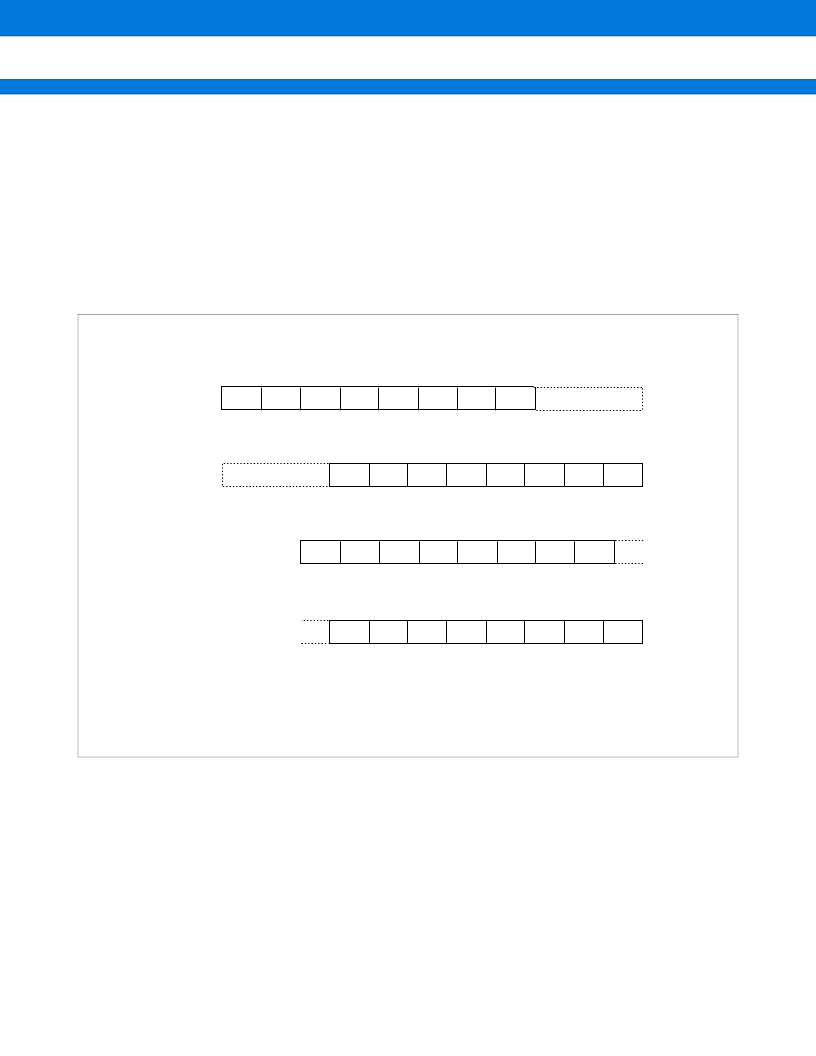
Register Configuration
—
—
—
CMOD OTE1
OTE0
OTD1
OTD0
(OCS0, OCS2)
OCU control status register ch.1, ch.3 (OCS1, OCS3)
bit 15
bit 14
bit 13
bit 12
bit 11
bit 10
bit 9
bit 8
bit 7. . . . . . . . . . . . .
—
—
—
R/W
R/W
R/W
R/W
R/W
Address
000063
H
000065
H
Initial value
- - -00000
B
ICP1
ICP0
ICE1
ICE0
—
—
CST1
CST0
(OCS1, OCS3)
OCU control status register ch.0, ch.2 (OCS0, OCS2)
bit 7
bit 6
bit 5
bit 4
bit 3
bit 2
bit 1
bit 0
bit 15. . . . . . . . . . . .
R/W
R/W
R/W
R/W
—
—
R/W
R/W
C15
C14
C13
C12
C11
C10
C09
C08
OCU compare register ch.0 to ch.3 (OCCP0 to OCCP3)
Address
OCCP0 (high order address): 00005B
H
OCCP1 (high order address): 00005D
H
OCCP2 (high order address): 00005F
H
OCCP3 (high order address): 000061
H
bit 15
bit 14
bit 13
bit 12
bit 11
bit 10
bit 9
bit 8
R/W
R/W
R/W
R/W
R/W
R/W
R/W
R/W
Initial value
XXXXXXXX
B
C07
C06
C05
C04
C03
C02
C01
C00
bit 7
bit 6
bit 5
bit 4
bit 3
bit 2
bit 1
bit 0
R/W
R/W
R/W
R/W
R/W
R/W
R/W
R/W
R/W : Readable and writable
— : Reserved
X : Undefined
Initial value
0000- -00
B
Address
000062
H
000064
H
Initial value
XXXXXXXX
B
Address
OCCP0 (low order address): 00005A
H
OCCP1 (low order address): 00005C
H
OCCP2 (low order address): 00005E
H
OCCP3 (low order address): 000060
H
相關(guān)PDF資料 |
PDF描述 |
|---|---|
| MB90F574PFF | 16-bit Proprietary Microcontroller |
| MB90F574PFV | 16-bit Proprietary Microcontroller |
| MB90573 | Hex Schmitt-trigger Inverters 14-CFP -55 to 125 |
| MB90573PFF | 16-bit Proprietary Microcontroller |
| MB90573PFV | 16-bit Proprietary Microcontroller |
相關(guān)代理商/技術(shù)參數(shù) |
參數(shù)描述 |
|---|---|
| MB90F583BPFR-GE1 | 制造商:FUJITSU 功能描述: |
| MB90F583BPMC-GE1 | 制造商:FUJITSU 功能描述: |
| MB90F583CAPFR-GE1 | 制造商:FUJITSU 功能描述: |
| MB90F591GPFR-GE1 | 制造商:FUJITSU 功能描述: |
| MB90F594APFR-GE1 | 制造商:FUJITSU 功能描述: |
發(fā)布緊急采購,3分鐘左右您將得到回復。