- 您現(xiàn)在的位置:買賣IC網(wǎng) > PDF目錄377927 > MB90F574A (Fujitsu Limited) Octal Bus Transceivers And Registers With 3-State Outputs 24-CFP -55 to 125 PDF資料下載
參數(shù)資料
| 型號: | MB90F574A |
| 廠商: | Fujitsu Limited |
| 英文描述: | Octal Bus Transceivers And Registers With 3-State Outputs 24-CFP -55 to 125 |
| 中文描述: | 16位微控制器專有 |
| 文件頁數(shù): | 9/135頁 |
| 文件大小: | 2504K |
| 代理商: | MB90F574A |
第1頁第2頁第3頁第4頁第5頁第6頁第7頁第8頁當前第9頁第10頁第11頁第12頁第13頁第14頁第15頁第16頁第17頁第18頁第19頁第20頁第21頁第22頁第23頁第24頁第25頁第26頁第27頁第28頁第29頁第30頁第31頁第32頁第33頁第34頁第35頁第36頁第37頁第38頁第39頁第40頁第41頁第42頁第43頁第44頁第45頁第46頁第47頁第48頁第49頁第50頁第51頁第52頁第53頁第54頁第55頁第56頁第57頁第58頁第59頁第60頁第61頁第62頁第63頁第64頁第65頁第66頁第67頁第68頁第69頁第70頁第71頁第72頁第73頁第74頁第75頁第76頁第77頁第78頁第79頁第80頁第81頁第82頁第83頁第84頁第85頁第86頁第87頁第88頁第89頁第90頁第91頁第92頁第93頁第94頁第95頁第96頁第97頁第98頁第99頁第100頁第101頁第102頁第103頁第104頁第105頁第106頁第107頁第108頁第109頁第110頁第111頁第112頁第113頁第114頁第115頁第116頁第117頁第118頁第119頁第120頁第121頁第122頁第123頁第124頁第125頁第126頁第127頁第128頁第129頁第130頁第131頁第132頁第133頁第134頁第135頁
9
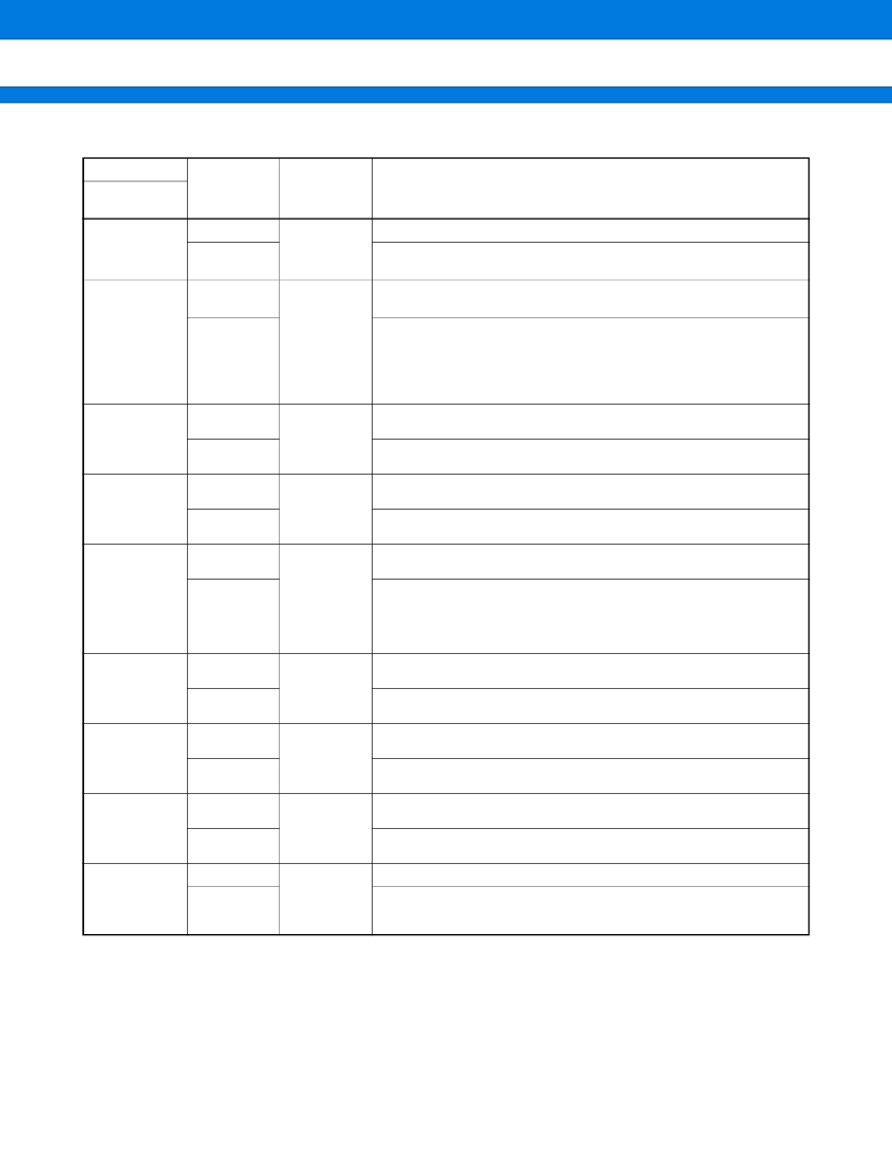
MB90570 Series
Pin no.
LQFP-120 *
1
QFP-120 *
2
7
Pin name
Circuit type
Function
P37
CLK
E
In single chip mode this is a general-purpose I/O port.
In external bus mode, this pin functions as the clock (CLK) signal output
pin.
In single chip mode this is a general-purpose I/O port. It can be set to open
drain by the ODR4 register.
This is also the UART ch.0 serial data input pin. While UART ch.0 is in
input operation, this input signal is in continuous use, and therefore the
output function should only be used when needed. If shared by output
from other functions, this pin should be output disabled during SIN
operation.
In single chip mode this is a general-purpose I/O port. It can be set to open
drain by the ODR4 register.
This is also the UART ch.0 serial data output pin. This function is valid
when UART ch.0 is enabled for data output.
In single chip mode this is a general-purpose I/O port. It can be set to open
drain by the ODR4 register.
This is also the UART ch.0 serial clock I/O pin. This function is valid when
UART ch.0 is enabled for clock output.
In single chip mode this is a general-purpose I/O port. It can be set to
open-drain by the ODR4 register.
This is also the UART ch.1 serial data input pin. While UART ch.1 is in
input operation, this input signal is in continuous use, and therefore the
output function should only be used when needed. If shared by output
from other functions, this pin should be output disabled during SIN
operation.
In single chip mode this is a general-purpose I/O port. It can be set to
opendrain by the ODR4 register.
This is also the UART ch.1 serial data output pin. This function is valid
when UART ch.1 is enabled for data output.
In single chip mode this is a general-purpose I/O port. It can be set to open
drain by the ODR4 register.
This is also the UART ch.1 serial clock I/O pin. This function is valid when
UART ch.1 is enabled for clock output.
In single chip mode this is a general-purpose I/O port. It can be set to open
drain by the ODR4 register.
These are also the PPG0, 1 output pins. This function is valid when PPG0,
1 output is enabled.
In single chip mode this is a general-purpose I/O port.
9
P40
F
SIN0
10
P41
F
SOT0
11
P42
F
SCK0
12
P43
F
SIN1
13
P44
F
SOT1
14
P45
F
SCK1
15,16
P46,P47
F
PPG0,PPG1
17
P50
SIN2
E
This is also the I/O serial ch.0 data input pin. During serial data input, this
input signal is in continuous use, and therefore the output function should
only be used when needed.
*1: FPT-120P-M05
*2: FPT-120P-M13
,
FPT-120P-M21
(Continued)
相關PDF資料 |
PDF描述 |
|---|---|
| MB90F574APMT | 16-bit Proprietary Microcontroller |
| MB90F574PFF | 16-bit Proprietary Microcontroller |
| MB90F574PFV | 16-bit Proprietary Microcontroller |
| MB90573 | Hex Schmitt-trigger Inverters 14-CFP -55 to 125 |
| MB90573PFF | 16-bit Proprietary Microcontroller |
相關代理商/技術參數(shù) |
參數(shù)描述 |
|---|---|
| MB90F583BPFR-GE1 | 制造商:FUJITSU 功能描述: |
| MB90F583BPMC-GE1 | 制造商:FUJITSU 功能描述: |
| MB90F583CAPFR-GE1 | 制造商:FUJITSU 功能描述: |
| MB90F591GPFR-GE1 | 制造商:FUJITSU 功能描述: |
| MB90F594APFR-GE1 | 制造商:FUJITSU 功能描述: |
發(fā)布緊急采購,3分鐘左右您將得到回復。