- 您現(xiàn)在的位置:買賣IC網(wǎng) > PDF目錄377927 > MB90F568PFM (FUJITSU LTD) 16-bit Proprietary Microcontrollers PDF資料下載
參數(shù)資料
| 型號(hào): | MB90F568PFM |
| 廠商: | FUJITSU LTD |
| 元件分類: | 微控制器/微處理器 |
| 英文描述: | 16-bit Proprietary Microcontrollers |
| 中文描述: | 16-BIT, FLASH, 16 MHz, MICROCONTROLLER, PQFP64 |
| 封裝: | 0.65 MM PITCH, PLASTIC, LQFP-64 |
| 文件頁(yè)數(shù): | 20/91頁(yè) |
| 文件大小: | 484K |
| 代理商: | MB90F568PFM |
第1頁(yè)第2頁(yè)第3頁(yè)第4頁(yè)第5頁(yè)第6頁(yè)第7頁(yè)第8頁(yè)第9頁(yè)第10頁(yè)第11頁(yè)第12頁(yè)第13頁(yè)第14頁(yè)第15頁(yè)第16頁(yè)第17頁(yè)第18頁(yè)第19頁(yè)當(dāng)前第20頁(yè)第21頁(yè)第22頁(yè)第23頁(yè)第24頁(yè)第25頁(yè)第26頁(yè)第27頁(yè)第28頁(yè)第29頁(yè)第30頁(yè)第31頁(yè)第32頁(yè)第33頁(yè)第34頁(yè)第35頁(yè)第36頁(yè)第37頁(yè)第38頁(yè)第39頁(yè)第40頁(yè)第41頁(yè)第42頁(yè)第43頁(yè)第44頁(yè)第45頁(yè)第46頁(yè)第47頁(yè)第48頁(yè)第49頁(yè)第50頁(yè)第51頁(yè)第52頁(yè)第53頁(yè)第54頁(yè)第55頁(yè)第56頁(yè)第57頁(yè)第58頁(yè)第59頁(yè)第60頁(yè)第61頁(yè)第62頁(yè)第63頁(yè)第64頁(yè)第65頁(yè)第66頁(yè)第67頁(yè)第68頁(yè)第69頁(yè)第70頁(yè)第71頁(yè)第72頁(yè)第73頁(yè)第74頁(yè)第75頁(yè)第76頁(yè)第77頁(yè)第78頁(yè)第79頁(yè)第80頁(yè)第81頁(yè)第82頁(yè)第83頁(yè)第84頁(yè)第85頁(yè)第86頁(yè)第87頁(yè)第88頁(yè)第89頁(yè)第90頁(yè)第91頁(yè)
MB90560/565 Series
20
I
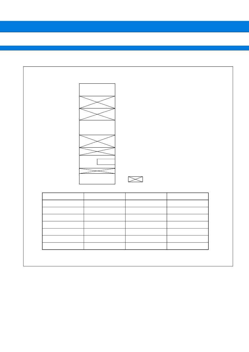
MEMORY MAP
Memory map of MB90560/565 series
Notes :
When specified in the ROM mirror function register, the upper part of 00 bank (“004000
H
to 00FFFF
H
”)
contains a mirror of the data in the upper part of FF bank (“FF4000
H
to FFFFFF
H
”) .
See “10. ROM Mirror Function Selection Module” in the Peripheral Functions section for details of the
ROM mirror function settings.
Remarks :
The ROM mirror function is provided so the C compiler’s small memory model can be used.
The lower 16 bits of the FF bank and 00 bank addresses are the same. However, as the FF bank ROM
area exceeds 48 KBytes, the entire ROM data area cannot be mirrored in 00 bank.
When using the C compiler’s small memory model, locating data tables in the area “FF4000
H
to
FFFFFF
H
” makes the image of the data visible in the “004000
H
to 00FFFF
H
” area. This means that
data tables located in ROM can be referenced without needing to declare far pointers.
FFFFFF
H
FF0000
H
010000
H
004000
H
000100
H
0000C0
H
000000
H
Single chip mode
(with ROM mirror function)
ROM area
Address #1
ROM area
(image of FF bank)
Address #2
Address #3
RAM
area
Registers
Peripherals
Access prohibited
* : “V” products do not contain internal ROM. Treat this address as the ROM decode area
used by the tools.
Part No.
Address#1
Address#2
Address#3
MB90561/A
FF8000
H
008000
H
000500
H
MB90562/A
FF0000
H
004000
H
000900
H
MB90F562/B
FF0000
H
004000
H
000900
H
MB90567
FE8000
H
004000
H
001100
H
MB90568
FE0000
H
004000
H
001100
H
MB90F568
FE0000
H
004000
H
001100
H
MB90V560
FE0000
H*
004000
H*
001100
H
相關(guān)PDF資料 |
PDF描述 |
|---|---|
| MB90F562BPFM | 16-bit Proprietary Microcontrollers |
| MB90F562P | 16-bit Proprietary Microcontrollers |
| MB90F562PF | 16-bit Proprietary Microcontrollers |
| MB90F562PFM | 16-bit Proprietary Microcontrollers |
| MB90F568 | 16-bit Proprietary Microcontrollers |
相關(guān)代理商/技術(shù)參數(shù) |
參數(shù)描述 |
|---|---|
| MB90F568PMCR-GE1 | 制造商:FUJITSU 功能描述: |
| MB90F583BPFR-GE1 | 制造商:FUJITSU 功能描述: |
| MB90F583BPMC-GE1 | 制造商:FUJITSU 功能描述: |
| MB90F583CAPFR-GE1 | 制造商:FUJITSU 功能描述: |
| MB90F591GPFR-GE1 | 制造商:FUJITSU 功能描述: |
發(fā)布緊急采購(gòu),3分鐘左右您將得到回復(fù)。